


D15343-003 5
Contents
4.10.9 SVID – Subsystem Vendor Identification Register.................................................97
4.10.10 ID – Subsystem Identification Register..................................................................97
4.10.11 CAPPTR – Capabilities Pointer Register...............................................................98
4.10.12 HPLLCC – HPLL Clock Control Register (Device #0) ...........................................98
4.11 Intel
®
82854 GMCH Integrated Graphics Device Registers (Device #2, Function #0).....100
4.11.1 VID – Vendor Identification Register (Device #2) ................................................101
4.11.2 DID – Device Identification Register (Device #2).................................................101
4.11.3 PCICMD – PCI Command Register (Device #2) .................................................102
4.11.4 PCISTS – PCI Status Register (Device #2).........................................................103
4.11.5 RID – Revision Identification Register (Device #2) ..............................................103
4.11.6 CC – Class Code Register (Device #2) ...............................................................104
4.11.7 CLS – Cache Line Size Register (Device #2) ......................................................104
4.11.8 MLT – Master Latency Timer Register (Device #2) .............................................104
4.11.9 HDR – Header Type Register (Device #2)...........................................................105
4.11.10 GMADR – Graphics Memory Range Address Register (Device #2)....................105
4.11.11 MMADR – Memory Mapped Range Address Register (Device #2).....................106
4.11.12 IOBAR – I/O Base Address Register (Device #2)................................................106
4.11.13 SVID – Subsystem Vendor Identification Register (Device #2) ...........................107
4.11.14 SID – Subsystem Identification Register (Device #2) ..........................................107
4.11.15 ROMADR – Video BIOS ROM Base Address Registers (Device #2)..................107
4.11.16 INTRLINE – Interrupt Line Register (Device #2)..................................................108
4.11.17 INTRPIN – Interrupt Pin Register (Device #2) .....................................................108
4.11.18 MINGNT – Minimum Grant Register (Device #2) ................................................108
4.11.19 MAXLAT – Maximum Latency Register (Device #2)............................................109
4.11.20 PMCAP – Power Management Capabilities Register (Device #2).......................109
4.11.21 PMCS – Power Management Control/Status Register (Device #2).....................110
5.0 Intel
®
82854 GMCH System Address Map..................................................................................111
5.1 System Memory Address Ranges ....................................................................................111
5.2 DOS Compatibility Area....................................................................................................112
5.3 Extended System Memory Area .......................................................................................114
5.4 Main System Memory Address Range (0010_0000h to Top of Main Memory)................115
5.4.1 15 MB-16 MB Window .........................................................................................115
5.4.2 Pre-allocated System Memory.............................................................................115
5.4.3 System Management Mode (SMM) Memory Range............................................118
5.4.4 System Memory Shadowing ................................................................................119
5.4.5 I/O Address Space...............................................................................................119
5.4.6 GMCH Decode Rules and Cross-Bridge Address Mapping ................................120
5.4.7 Hub Interface Decode Rules................................................................................121
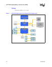
6.0 Functional Description .................................................................................................................123
6.1 Host Interface Overview ...................................................................................................123
6.2 Dynamic Bus Inversion .....................................................................................................123
6.2.1 System Bus Interrupt Delivery .............................................................................123
6.2.2 Upstream Interrupt Messages .............................................................................124
6.3 System Memory Interface.................................................................................................124
6.3.1 DDR SDRAM Interface Overview ........................................................................124
6.3.2 System Memory Organization and Configuration ................................................124
6.3.3 DDR SDRAM Performance Description...............................................................125
6.4 Integrated Graphics Overview ..........................................................................................126