


Intel
®
82854 Graphics Memory Controller Hub (GMCH)
104 D15343-003
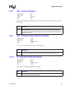
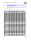
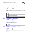
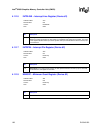
4.11.6 CC – Class Code Register (Device #2)
This register contains the device programming interface information related to the Sub-Class code
and Base Class code definition for the IGD. This register also contains the Base Class code and the
function sub-class in relation to the Base Class code.
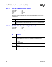
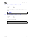
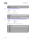
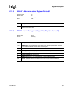
4.11.7 CLS – Cache Line Size Register (Device #2)
The IGD does not support this register as a PCI slave.
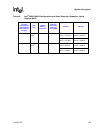
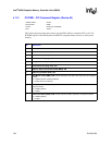
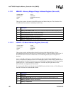
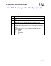
4.11.8 MLT – Master Latency Timer Register (Device #2)
The IGD does not support the programmability of the master latency timer because it does not
perform bursts.
Address Offset:
Default Value:
Access:
Size:
09-0Bh
030000h
Read Only
24 bits
Bit Description
23:16 Base Class Code (BASEC): 03=Display controller
15:8 Sub-Class Code (SCC):
Function 0: 00h=VGA compatible or 80h=Non VGA
Function 1: 80h=Non VGA
7:0 Programming Interface (PI): 00h=Hardwired as a Display controller.
Address Offset:
Default Value:
Access:
Size:
0Ch
00h
Read Only
8 bits
Bit Description
7:0 Cache Line Size (CLS) – RO
Address Offset:
Default Value:
Access:
Size:
0Dh
00h
Read Only
8 bits