


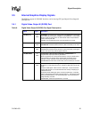
Signal Description
D15343-003 31
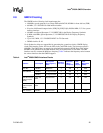
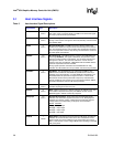
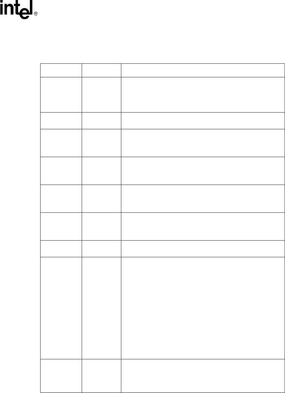
3.2 DDR SDRAM Interface
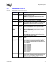
Table 6. DDR SDRAM Interface Descriptions
Signal Name Type Description
SCS[3:0]# O
SSTL_2
Chip Select: These pins select the particular DDR SDRAM
components during the active state.
NOTE: There is one SCS# per DDR-SDRAM Physical DDR DIMM
device row. These signals can be toggled on every rising System
Memory Clock edge (SCMDCLK).
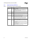
SMA[12:0] O
SSTL_2
Multiplexed Memory Address: These signals are used to provide the
multiplexed row and column address to the DDR SDRAM.
SBA[1:0] O
SSTL_2
Bank Select (Memory Bank Address): These signals define which
banks are selected within each DDR SDRAM row. The SMA and SBA
signals combine to address every possible location within a DDR
SDRAM device.
SRAS# O
SSTL_2
DDR Row Address Strobe: SRAS# may be heavily loaded and
requires tw0 DDR SDRAM clock cycles for setup time to the DDR
SDRAMs. Used with SCAS# and SWE# (along with SCS#) to define the
system memory commands.
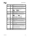
SCAS# O
SSTL_2
DDR Column Address Strobe: SCAS# may be heavily loaded and
requires two clock cycles for setup time to the DDR SDRAMs. Used
with SRAS# and SWE# (along with SCS#) to define the system memory
commands.
SWE# O
SSTL_2
Write Enable: Used with SCAS# and SRAS# (along with SCS#) to
define the DDR SDRAM commands. SWE# is asserted during writes to
DDR SDRAM. SWE# may be heavily loaded and requires two clock
cycles for setup time to the DDR SDRAMs.
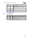
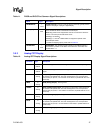
SDQ[63:0] I/O
SSTL_2
Data Lines: These signals are used to interface to the DDR SDRAM
data bus.
SDQS[8:0]
I/O
SSTL_2
Data Strobes: Data strobes are used for capturing data. During writes,
SDQS is centered on data. During reads, SDQS is edge aligned with
data. The following list matches the data strobe with the data bytes.
There is an associated data strobe (DQS) for each data signal (DQ) and
check bit (CB) group.
SDQS[7] -> SDQ[63:56]
SDQS[6] -> SDQ[55:48]
SDQS[5] -> SDQ[47:40]
SDQS[4] -> SDQ[39:32]
SDQS[3] -> SDQ[31:24]
SDQS[2] -> SDQ[23:16]
SDQS[1] -> SDQ[15:8]
SDQS[0] -> SDQ[7:0]
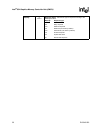
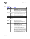
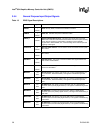
SCKE[3:0] O
SSTL_2
Clock Enable: These pins are used to signal a self-refresh or power
down command to the DDR SDRAM array when entering system
suspend. SCKE is also used to dynamically power down inactive DDR
SDRAM rows. There is one SCKE per DDR SDRAM row. These
signals can be toggled on every rising SCK edge.