


Intel
®
82854 Graphics Memory Controller Hub (GMCH)
144 D15343-003
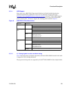
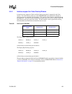
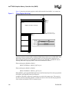
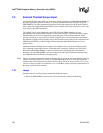
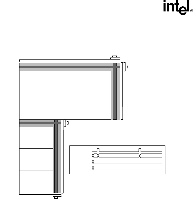
Figure 11 shows how the timing registers switch while the buffer 0 and buffer 1 are scanned out.
As shown in the above figure, buffer switching in Multi-display mode occurs on VBLANK. Once
VBLANK is detected, horizontal and vertical counters are reset and register switching occurs.
These operations result in an extended HSYNC following the VBLANK. The HSYNC interval
following VBLANK rising edge in MTV mode can be calculated as follows:
When switching from Buffer0 to Buffer1:
HSYNC INTERVAL = HSYNC_B[27:16] + 8
When switching from Buffer1 to Buffer0:
HSYNC INTERVAL = HSYNC_A[27:16] + 8
Where HSYNC_A[27:16] and HSYNC_B[27:16] are the Horizontal Sync End values programmed
in the PipeA and PipeB Horizontal Sync Registers.
In addition, VBLANK is effectively started twice as a result of the counter reset. This results in
two lines of inactive data being repeated. VSYNC will start two lines later then the programmed
value, and the total number of lines is extended by two.
Figure 11. Timing Register Switching
MP@ML 720x480(i) / 720x480(p)
Buffer 0
timing register switching
occurs on VBLANK rising edge
Buffer 1
VTOTAL_A
HSYNC_A
VBLANK_A
VSYNC_A
VBLANK_B
VSYNC_B
VTOTAL_B
HTOTAL_A
HBLANK_A
HTOTAL_B
HBLANK_B
HSYNC_B
04650438h
062705A0h
04650438h 062705A0h
VBLANK
VTOTAL
VTOTAL_A
VTOTAL_B