


Intel
®
82854 GMCH Overview
D15343-003 25
2.8 GMCH Clocking
The GMCH has the following clock input/output pins:
• 400-MHz, spread spectrum, low voltage differential BCLK, BCLK# for front side bus (FSB)
• 66-MHz, 3.3-V GCLKIN for Hub interface buffers
• Six pairs of differential output clocks (SCK[5:0], SCK[5:0]#), 200/266 MHz, 2.5 V for system
memory interface
• 48-MHz, non-Spread Spectrum, 3.3-V DREFCLK for the Display Frequency Synthesis
• 8-MHz or 66-MHz, Spread Spectrum, 3.3-V DREFSSCLK for the Display Frequency
Synthesis
• Up to 148.5 MHz, 1.5-V DVOBCCLKINT for TV-Out mode
• DPMS clock for S1-M
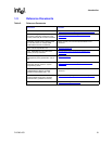
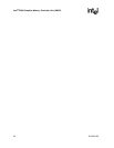
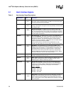
Clock Synthesizer chips are responsible for generating the system host clocks, GMCH display
clocks, Hub interface clocks, PCI clocks, SIO clocks, and FWH clocks. The host target speed is
400 MHz. The GMCH does not require any relationship between the BCLK Host clock and the
66-MHz clock generated for the Hub interface; they are asynchronous to each other. The Hub
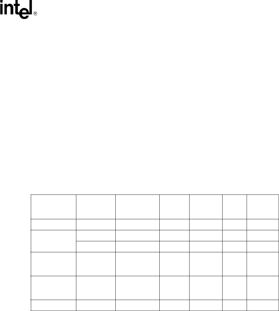
interface runs at a constant 66-MHz base frequency. Table 4 indicates the frequency ratios between
the various interfaces that the GMCH supports.
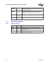
Table 4. Intel
®
82854 GMCH Interface Clocks
Interface Clock Speed
CPU System
Bus Frequency
Ratio
Samples
Per Clock
Data Rate
(Mega-
samples/s)
Data
Width
(Bytes)
Peak
Bandwidth
(MB/s)
CPU Bus 100 MHz Reference 4 400 8 3200
DDR SDRAM 133 MHz 1:1 Synchronous 2 266 8 2128
166 MHz 1:1 Synchronous 2 333 8 2664
DVO B or DVO C
(Native Graphic
Mode)
Up to 165
MHz
Asynchronous 2 330 1.5 495
DVO B+DVO C
(Native Graphic
Mode)
Up to 330
MHz
Asynchronous 2 660 3 1980
DAC Interface 350 MHz Asynchronous 1 350 3 1050