


Intel
®
82854 Graphics Memory Controller Hub (GMCH)
80 D15343-003
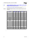
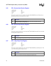
4.9.14 DRT – DRAM Timing Register (Device #0)
This register controls the timing of the DDR SDRAM controller.
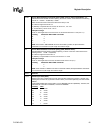
Address Offset:
Default Value:
Access:
Size:
60-63h
18004425h
Read/Write
32 bits
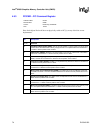
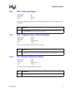
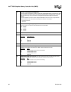
Bit Description
31 DDR Internal Write to Read Command delay (tWTR):
The tWTR is a std. DDR SDRAM timing parameter with a value of 1 CK for CL=2 and 2.5. The
tWTR is used to time RD command after a WR command (to same Row):
0: tWTR is set to 1 Clock (CK), used for DDR SDRAM CL=2 or 2.5
1: Reserved
30 DDR Write Recovery time (tWR):
Write recovery time is a std. DDR timing parameter with the value of 15 ns. It should be set to 2 CK
when DDR200 is used. The tWR is used to time PRE command launch after a WR command,
when DDR SDRAM components are populated.
0: tWR is set to 2 Clocks (CK)
1: tWR is set to 3 Clocks (CK)
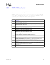
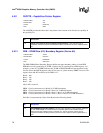
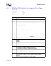
29:28 Back To Back Write-Read commands spacing (DDR different Rows/Bank
):
This field determines the WR-RD command spacing, in terms of common clocks for DDR SDRAM
based on the following formula: DQSS + 0.5xBL + TA (WR-RD) – CL
DQSS: is time from Write command to data and is always 1 CK
BL: is Burst Length and can be set to 4.
TA (WR-RD): is required DQ turn-around, can be set to 1 or 2 CK
CL: is CAS Latency, can be set to 2 or 2.5
Examples of usage:
For BL=4, with single DQ turn-around and CL=2, this field must be set to 2 CK (1+2+1-2)
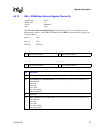
Encoding CK between WR and RD commands
00: 4
01: 3
10: 2
11: Reserved