


Register Description
D15343-003 109
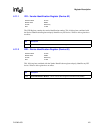
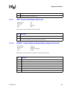
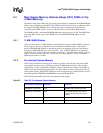
4.11.19 MAXLAT – Maximum Latency Register (Device #2)
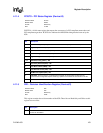
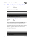
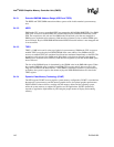
4.11.20 PMCAP – Power Management Capabilities Register (Device #2)
Address Offset:
Default Value:
Access:
Size:
3Fh
00h
Read Only
8 bits
Bit Description
7:0 Maximum Latency Value: Bits[7:0]=00h. The IGD has no specific requirements for how often it
needs to access the PCI bus.
Address Offset:
Default Value:
Access:
Size:
D2-D3h
0221h
Read Only
16 bits
Bit Description
15:11 PME Support: This field indicates the power states in which the IGD may assert PME#. Hardwired
to 0 to indicate that the IGD does not assert the PME# signal.
10:6 Reserved
5 Device Specific Initialization (DSI): Hardwired to 1 to indicate that special initialization of the IGD
is required before generic class device driver is to use it.
4 Auxiliary Power Source: Hardwired to 0.
3 PME Clock: Hardwired to 0 to indicate IGD does not support PME# generation.
2:0 Version: Hardwired to 001b to indicate there are 4 bytes of power management registers
implemented.