


D15343-003 3
Contents
Contents
1.0 Introduction....................................................................................................................................11
1.1 Overview.............................................................................................................................11
1.2 Terminology ........................................................................................................................17
1.3 Reference Documents ........................................................................................................19
2.0 Intel
®
82854 GMCH Overview.......................................................................................................21
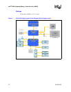
2.1 System Architecture............................................................................................................21
2.1.1 Intel
®
82854 GMCH ...............................................................................................21
2.2 Processor Host Interface ....................................................................................................22
2.3 GMCH System Memory Interface.......................................................................................22
2.4 Graphics Features ..............................................................................................................23
2.5 Display Features.................................................................................................................23
2.5.1 GMCH Analog Display Port ...................................................................................23
2.5.2 GMCH Integrated DVO Ports ................................................................................23
2.6 Hub Interface ......................................................................................................................24
2.7 Address Decode Policies....................................................................................................24
2.8 GMCH Clocking ..................................................................................................................25
2.9 System Interrupts................................................................................................................26
3.0 Signal Description..........................................................................................................................27
3.1 Host Interface Signals.........................................................................................................28
3.2 DDR SDRAM Interface .......................................................................................................31
3.3 Hub Interface Signals .........................................................................................................32
3.4 Clocks .................................................................................................................................33
3.5 Internal Graphics Display Signals.......................................................................................35
3.5.1 Digital Video Output B (DVOB) Port ......................................................................35
3.5.2 Digital Video Output C (DVOC) Port...................................................................... 36
3.5.3 Analog CRT Display ..............................................................................................37
3.5.4 General Purpose Input/Output Signals ..................................................................38
3.6 Voltage References, PLL Power.........................................................................................39
4.0 Register Description ......................................................................................................................41
4.1 Conceptual Overview of the Platform Configuration Structure ...........................................41
4.2 Nomenclature for Access Attributes ...................................................................................42
4.3 Standard PCI Bus Configuration Mechanism .....................................................................43
4.4 Routing Configuration Accesses.........................................................................................43
4.4.1 PCI Bus #0 Configuration Mechanism...................................................................43
4.4.2 Primary PCI and Downstream Configuration Mechanism......................................44
4.5 Register Definitions.............................................................................................................44
4.6 I/O Mapped Registers.........................................................................................................45
4.6.1 CONFIG_ADDRESS – Configuration Address Register........................................45
4.6.2 CONFIG_DATA – Configuration Data Register.....................................................47
4.7 VGA I/O Mapped Registers ................................................................................................48
4.8 Intel 854 GMCH Host-Hub Interface Bridge Device Registers (Device #0, Function #0) ...49
4.8.1 VID – Vendor Identification Register......................................................................51
4.8.2 DID – Device Identification Register ......................................................................51
4.8.3 PCICMD – PCI Command Register.......................................................................52