


Register Description
D15343-003 87
6:4 Mode Select (SMS). These bits select the special operational mode of the DDR SDRAM
Interface. The special modes are intended for initialization at power up.
000: Post Reset State – When the GMCH exits Reset (power-up or otherwise), the mode select
field is cleared to 000. Software is not expected to Write this value, however if this value is Written,
there are no side effects (no Self Refresh or any other special DDR SDRAM cycle).
During any Reset sequence, while power is applied and Reset is active, the GMCH deasserts all
CKE signals. After internal Reset is deasserted, CKE signals remain deasserted until this field is
written to a value different than 000. On this event, all CKE signals are asserted.
During Suspend (S3, S4), GMCH internal signal triggers DDR SDRAM Controller to flush pending
commands and enter all rows into Self-Refresh mode. As part of Resume sequence, GMCH will
be Reset , which will clear this bit field to 000 and maintain CKE signals deasserted. After internal
Reset is deasserted, CKE signals remain deasserted until this field is Written to a value different
than 000. On this event, all CKE signals are asserted.
During Entry to other low power states (C3, S1-M), GMCH internal signal triggers DDR SDRAM
Controller to flush pending commands and enter all rows in S1 and relevant rows in C3 (Based on
RPDNC3) into Self-Refresh mode. During exit to Normal mode, the GMCH signal triggers DDR
SDRAM Controller to Exit Self-Refresh and Resume Normal operation without S/W involvement.
001: NOP Command Enable – All CPU cycles to DDR SDRAM result in a NOP command on the
DDR SDRAM interface.
010: All Banks Pre-charge Enable – All CPU cycles to DDR SDRAM result in an All Banks
Precharge command on the DDR SDRAM interface.
011: Mode Register Set Enable – All CPU cycles to DDR SDRAM result in a Mode Register set
command on the DDR SDRAM Interface. Host address lines are mapped to DDR SDRAM
address lines in order to specify the command sent. Host address HA[13:3] are mapped to
Memory address SMA[11,9:0]. SMA3 must be driven to 1 for interleave wrap type.
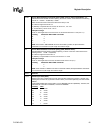
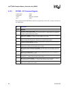
For Double Data Rate
MA[6:4] needs to be driven based on the value programmed in the CAS# Latency field.
CAS Latency
MA[6:4]
1.5 Clocks 001
2.0 Clocks 010
2.5 Clocks 110
SMA[7] should always be driven to a 0.
SMA[8] Should be driven to a 1 for DLL Reset and 1 for Normal Operation.
SMA[12:9] must be driven to 00000.
BIOS must calculate and drive the correct host address for each row of Memory such that the
correct command is driven on the SMA[12:0] lines. Note that SMAB[5,4,2,1]# are inverted from
SMA[5,4,2,1]; BIOS must account for this.
100: Extended Mode Register Set Enable – All CPU cycles to DDR SDRAM result in an
“Extended Mode register set” command on the DDR SDRAM Interface. Host address lines are
mapped to DDR SDRAM address lines in order to specify the command sent. Host address lines
are mapped to DDR SDRAM address lines in order to specify the command sent. Host address
HA[13:3] are mapped to Memory address SMA[11,9:0]. SMA[0] = 0 for DLL enable and 1 for DLL
disable. All the other SMA lines are driven to 0’s. Note that SMAB[5,4,2,1]# are inverted from
SMA[5,4,2,1]; BIOS must account for this.
101: Reserved
110: CBR Refresh Enable – In this mode all CPU cycles to DDR SDRAM result in a CBR cycle on
the DDR SDRAM interface
111: Normal operation
3:0 Reserved