


Signal Description
D15343-003 33
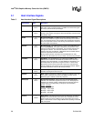
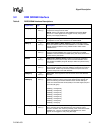
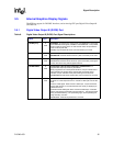
3.4 Clocks
Table 8. Clock Signals
Signal Name Type Description
Host Processor Clocking
BCLK
BCLK#
I
CMOS
Differential Host Clock In: These pins receive a buffered host clock
from the external clock synthesizer. This clock is used by all of the
GMCH logic that are in the Host clock domain (Host, Hub and system
memory). The clock is also the reference clock for the graphics core
PLL. This is a low voltage differential input.
System Memory Clocking
SCK[5:0] O
SSTL_2
Differential DDR SDRAM Clock: SCK and SCK# pairs are differential
clock outputs. The crossing of the positive edge of SCK and the
negative edge of SCK# is used to sample the address and control
signals on the DDR SDRAM. There are 3 pairs to each DDR DIMM.
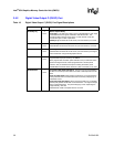
SCK[5:0]# O
SSTL_2
Complementary Differential DDR SDRAM Clock: These are the
complimentary differential DDR SDRAM clock signals.
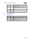
DVO/Hub Input Clocking
GCLKIN I
CMOS
Input Clock: 66-MHz, 3.3-V input clock from external buffer DVO/Hub
interface.
DVO Clocking
DVOBCLK
DVOBCLK#
O
DVO
Differential DVO Clock Output: These pins provide a differential pair
reference clock that can run up to 165-MHz.
DVOBCLK corresponds to the primary clock out.
DVOBCLK# corresponds to the primary complementary clock out.
DVOBCLK and DVOBCLK# should be left as NC (“Not Connected”) if
the DVO B port is not implemented.
DVOCCLK
DVOCCLK#
O
DVO
Differential DVO Clock Output: These pins provide a differential pair
reference clock that can run up to 165-MHz.
DVOCCLK corresponds to the primary clock out.
DVOCCLK# corresponds to the primary complementary clock out.
DVOCCLK and DVOCCLK# should be left as NC (“Not Connected”) if
the DVO C port is not implemented.
DVOBCCLKINT I
DVO
DVOBC Pixel Clock Input/Interrupt: This signal may be selected as
the reference input to either dot clock PLL (DPLL) or may be
configured as an interrupt input. A TV-out device can provide the clock
reference. The maximum input frequency for this signal is 148.5 -MHz.
DVOBC Pixel Clock Input: When selected as the dot clock PLL (DPLL)
reference input, this clock reference input supports SSC clocking for
DVO LVDS devices.
DVOBC Interrupt: When configured as an interrupt input, this interrupt
can support either DVOB or DVOC.
DVOBCCLKINT needs to be pulled down if the signal is NOT used.