Chapter 7 Wiring Diagrams and Signal Information
7-397
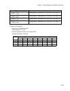
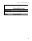
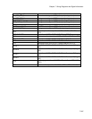
Signal line name Description
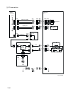
HV_REF_BTR_P Current control signal of BTR (+) output (analog value)
HV_REF_BTR_M Voltage control signal of BTR (–) output (analog value)
HV_REF_DTS Voltage control signal of DTS output (analog value)
BTR_P ON(L)+24VDC Voltage monitor signal of BTR(+) output (analog value)
BTR_M ON(L)+24VDC Voltage monitor signal of BTR(–) output (analog value)
DTS ON(L)+24VDC ON/OFF control signal of DTS output
HV_MONI_BTR_V Voltage monitor signal of BTR output (analog value)
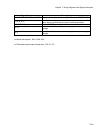
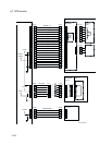
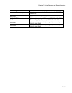
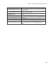
IDT2
Secondary transfer output from HVPS in PWBA HNB MCU to
IDT2
IDT2 CLEANER Output from HVPS in PWBA HNB MCU to IDT2 Cleaner
IDT1 Primary transfer output from HVPS in PWBA HNB MCU to IDT1
IDT1 CLEANER Output from HVPS in PWBA HNB MCU to IDT1 Cleaner
RFB Output from HVPS in PWBA HNB MCU to Refresher
RTC Charging output from HVPS in PWBA HNB MCU to RTC
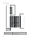
DEVE Y
Output from HVPS in PWBA HNB MCU to Developer Y(Magnet
Roll)
DEVE M
Output from HVPS in PWBA HNB MCU to Developer M(Magnet
Roll)
DEVE C
Output from HVPS in PWBA HNB MCU to Developer C(Magnet
Roll)
DEVE K
Output from HVPS in PWBA HNB MCU to Developer K(Magnet
Roll)
DTS
Discharging output from S-HVPS to Detack Saw in BTR UNIT
ASSY
BTR Third transfer output from S-HVPS to BTR in BTR UNIT ASSY


