


R61509V Target Spec
Rev. 0.11 April 25, 2008, page 104 of 181
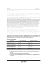
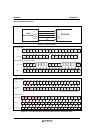
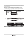
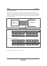
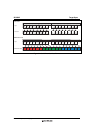
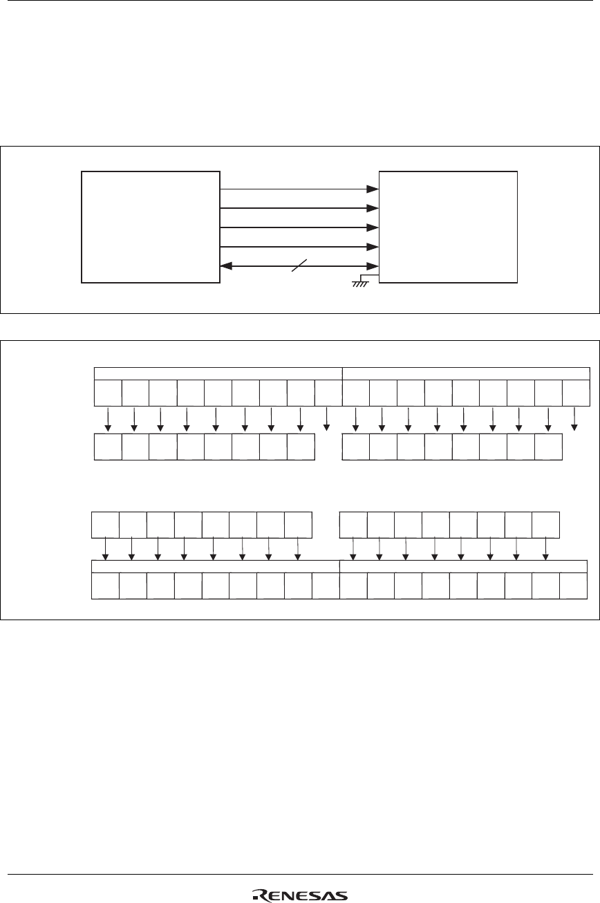
80-System 9-bit Bus Interface
When transferring 16-bit instruction, it is divided into upper and lower 8 bits, and the upper 8 bits are
transferred first (the LSB is not used). The RAM write data is also divided into upper and lower 9 bits, and
the upper 9 bits are transferred first. The unused DB pins must be fixed at either IOVCC or IOGND level.
When transferring the index register setting, make sure to write upper byte (8 bits).
A1
HWR
RS
WR:
9
9
R61509V
HOST
PROCESSOR
IM[2:0] = 001
CSn
(RDX) (RD:)
D15-0
CS:
DB17-9
DB8-0
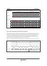
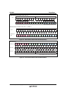
Figure 22 9-bit Interface
DB
17
DB
16
DB
15
DB
14
DB
13
DB
12
DB
11
DB
10
DB
9
DB
17
DB
16
DB
15
DB
14
DB
13
DB
12
DB
11
DB
10
DB
9
IB
15
IB IB
13
IB
12
IB
11
IB
10
IB
9
IB
8
IB
7
IB
6
IB
5
IB
4
IB
3
IB
2
IB
1
IB
014
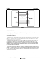
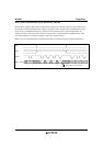
Instruction write
Input
Instruction
First transfer Second transfer
Instruction code
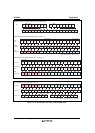
DB
17
DB
16
DB
15
DB
14
DB
13
DB
12
DB
11
DB
10
DB
9
DB
17
DB
16
DB
15
DB
14
DB
13
DB
12
DB
11
DB
10
DB
9
IB
15
IB IB
13
IB
12
IB
11
IB
10
IB
9
IB
8
IB
7
IB
6
IB
5
IB
4
IB
3
IB
2
IB
1
IB
0
14
First transfer Second transfer
Device code read / Instruction read
Instruction
Output
instruction code
Figure 23 9-bit Interface Data Format (Instruction Write / Device Code Read / Instruction Read)