R61509V Target Spec
Rev. 0.11 April 25, 2008, page 111 of 181
D0
LSB
1
“0” “1” “1” “1” “0” ID RS RW D15 D14 D13 D12 D11 D10 D9 D8 D7 D6 D5 D4 D3 D2 D1
2
3 4 5 6 7 8 9101112131415161718192021222324
Device ID code
RS RW
MSB
Transfer start
End of transfe
r
D0D15 D14 D13 D12 D11 D10 D9 D8 D7 D6 D5 D4 D3 D2 D1
Start byte
Instruction (1)
Upper 8 bits
Instruction (1)
Lower 8 bits
Instruction
execution time (1)
Dummy read
1
Dummy read
2
Dummy read
3
Dummy read
4
Dummy read
5
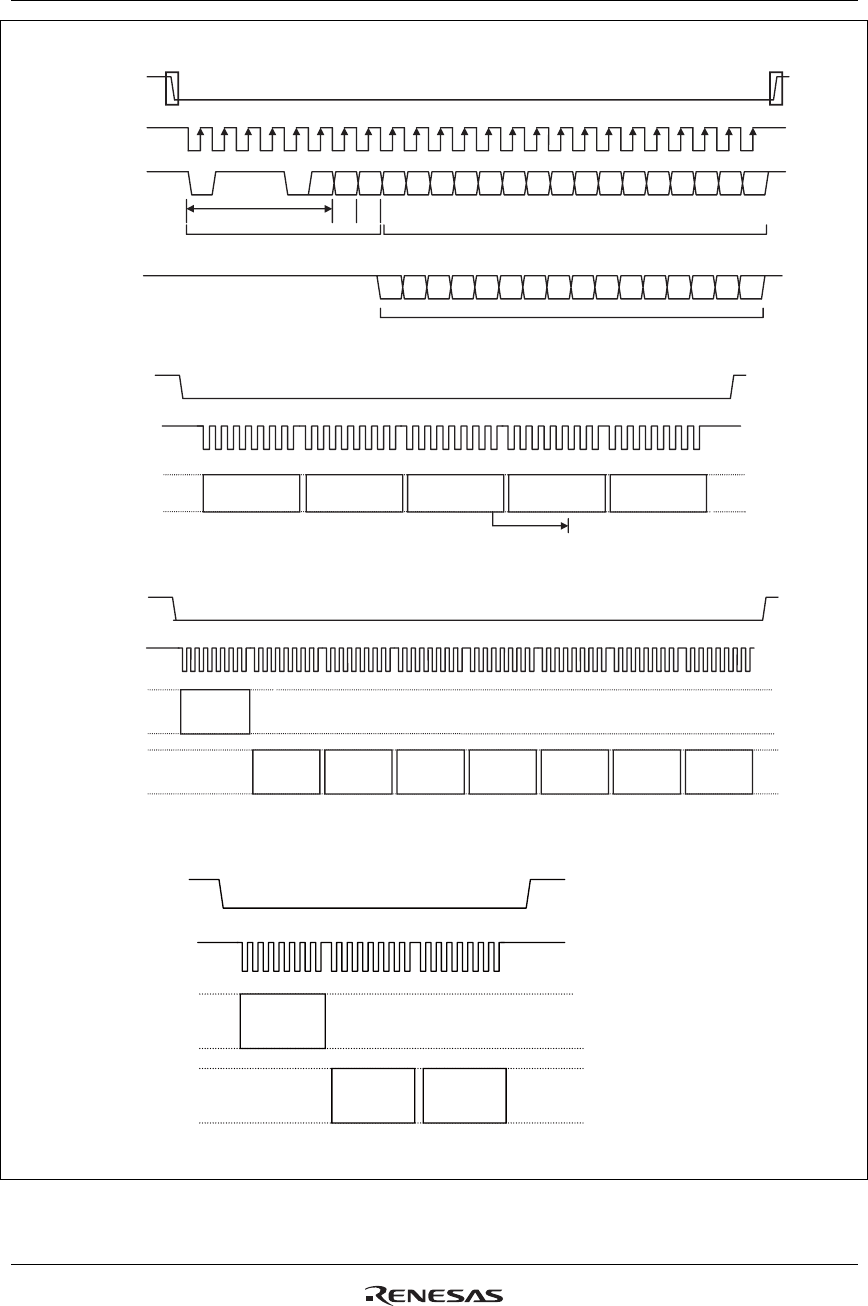
(a) Clock synchronization serial data transfer (basic mode)
(b) Clock synchronization serial consecutive data transfer
(c) RAM read data transfer
Instruction rea
d
L
ower
8
bits
Note: The eight bits read after start byte input is recognized
as the upper byte of instruction.
Note: Valid data is not sent until the R61509V reads five bytes from the GRAM after start byte input .
The R61509V sends valid data when it reads the sixth and subsequent bytes.
RAM read
Upper 8 bits
RAM read
Lower 8 bits
CSX
input
SCL
input
SDI
input
SDO
output
Start
End
CSX
input
SCL
input
SDI
input
CSX
input
SCL
input
SDI
input
SDO
output
Start
End
Instruction (2)
Upper 8 bits
Instruction (2)
Lower 8 bits
Read instruction, RAM data
Set IR (index register), instruction, write RAM data
Start byte
RS = 1
R/W = 1
Start byte
RS=0
R/W=1
CSX
input
SCL
input
SDI
input
SDO
output
Start byte
Instruction read
Upper 8 bits
Instruction read
Lower 8 bits
Start
End
(d) Instruction read
Note: Valid RAM data is read out right after the start byte.
Figure 32 Data Transfer in Serial Interface


