


R61509V Target Spec
Rev. 0.11 April 25, 2008, page 77 of 181
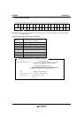
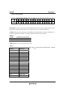
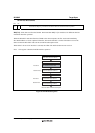
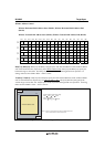
GRAM Data Read (R202h)
R/W RS
R 1
RAM read data RD[17:0] is transferred via different data bus in different interface operation.
RD[17:0]: 18-bit data read from the GRAM. RAM read data RD[17:0] is transferred via different data bus
in different interface operation.
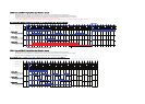
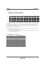
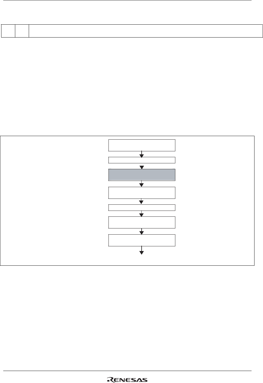
When the R61509V reads data from the GRAM to the microcomputer, the first word read immediately
after RAM address set is not outputted. Therefore, data on the data bus is invalid. Valid data is sent to the
data bus when the R61509V reads out the second and subsequent words.
When either 8-bit or 16-bit interface is selected, the LSBs of R and B dot data are not read out.
Note: This register is disabled in RGB interface operation
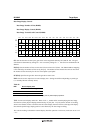
First word
Second word
First word
Second word
Set ID, AM,
HSA, HEA, VSA, and VEA bits
Set address N
Dummy read (invalid data to DB17-0)
From GRAM to read data latch
Set address M
Dummy read (invalid data to DB17-0)
From GRAM to read data latch
Read (data of address M)
From read data latch to DB17-0
Read out data to the microcompute
r
Read (data of address N)
From read data latch to DB17-0
Figure 8 GRAM Read Sequence