R61509V Target Spec
Rev. 0.11 April 25, 2008, page 158 of 181
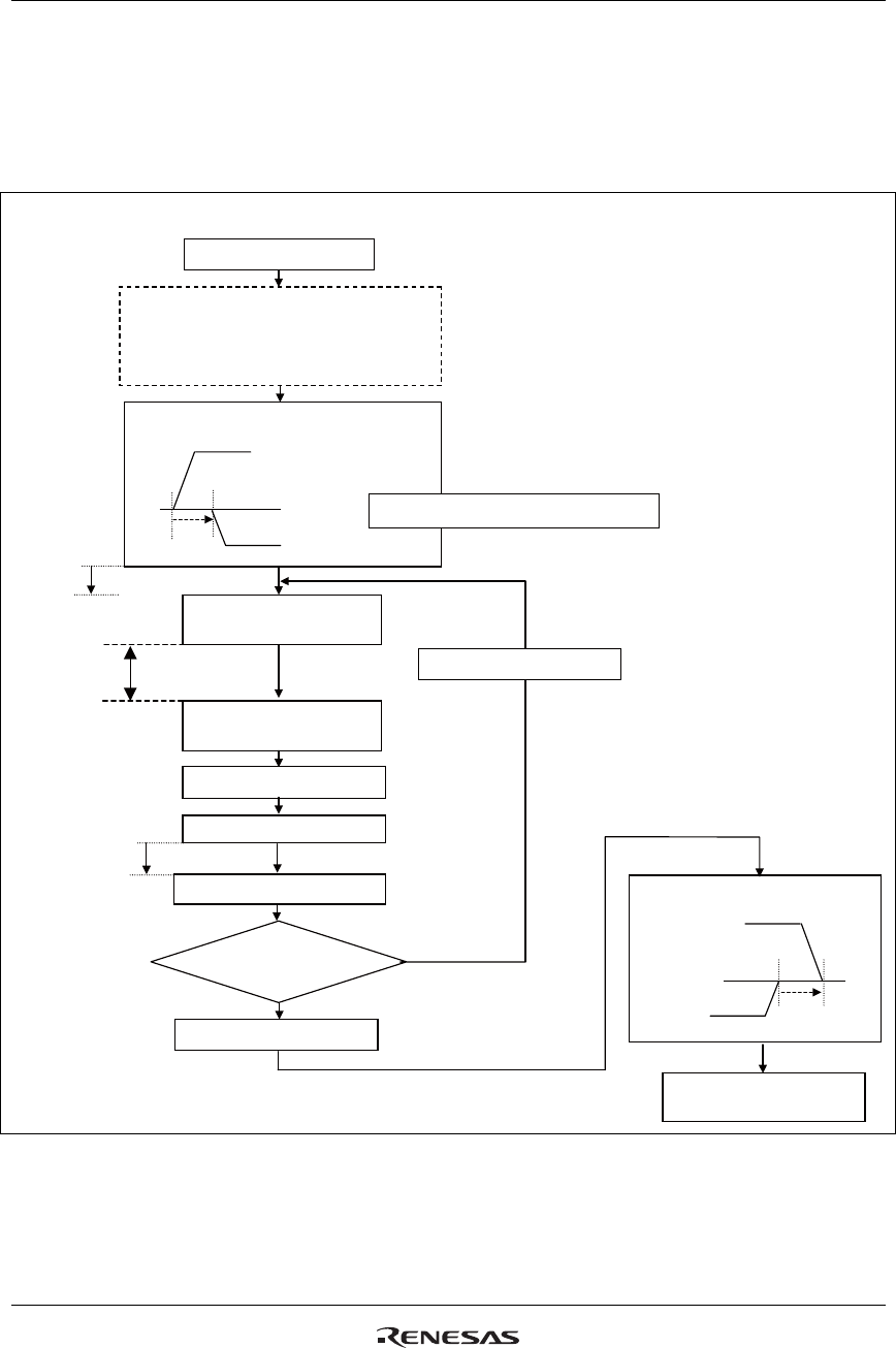
NVM Erase Sequence
The data written to the selected 16 bits is erased all together. The bits from which data is erased are set to
“1”. To erase data from NVM, make sure VGL
<
VPP3A, and follow the sequence below after power
supply ON sequence.
㩷
㩷
㩷
㩷
㩷
㩷㩷
㪩㪍㪝㪇㪿
㪚㪘㪣㪙
㪔
㪈
㩷
㩷
NVM Erase Sequence
Power supply OFF
sequence
1ms or more
NVM erase power supply setting
To erase data from NVM, set the VC and BT bits
as follows to make sure VGL < VPP3A < -9.5V.
(R100h): BT[2:0] = 3’h6 (VGL = -10.8V)
(R101h): VC[2:0] = 3’h7 (VCI = 2.7V)
Power supply ON sequence
Fix VPP3B to GND.
Erase period
10ms±1ms
NVM power supply ON
NVM power supply OFF
1ms
or more
1ms
or more
1ms or more
VPP1 = 9.2±0.3V
VPP3A = -9.2±0.3V
GND
GND
R6F0h:
TE=1, EOP[1:0]=2’h03
R6F0h:
TE=0, EOP[1:0]=2’h00
R6F2h: NVVRF=1
R280h: NVM data read
R6F2h: NVVRF=0
VPP1 = 9.2±0.3V
VPP3 = -9.2±0.3V
NVM data read result:
15’h7FFF
NO
YES
Verify OFF
Verify ON
Start of rasing
End of erasing
R6F2h: NVVRF=0
Figure 68 NVM Erase Sequence


