


R61509V Target Spec
Rev. 0.11 April 25, 2008, page 176 of 181
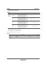
Note 3: Test 1, 2 and 3 pins must be grounded. The VDDTEST and VREFC must be fixed to AGND. The
IM0_ID pin must be fixed to IOVCC or be grounded.
Note 4: This excludes the current in the output drive MOS.
Note 5: This excludes the current in the input/output lines. Make sure that the input level is fixed because
through current will increase in the input circuit when the CMOS input level takes a middle range
level. The current consumption is unaffected by whether the CSX pin is high or low while not
accessing via interface pins.
Note 7: The output voltage deviation is the difference in the voltages from adjacent source pins for the
same display area. This value is shown for reference.
Note 8: The average output voltage dispersion is the variance source-output voltage of different chips of the
same product. The average source output voltage is measured for each chip with same display area.
Note 9: This applies to internal oscillators when using an internal RC oscillator.
Note 10: The liquid crystal driver output delay time depends on the load on the liquid crystal panel. Adjust
the frame frequency and the cycle per line by checking the quality of display on the actual panel in
use.
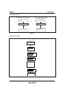
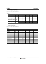
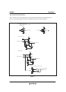
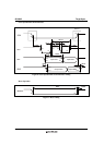
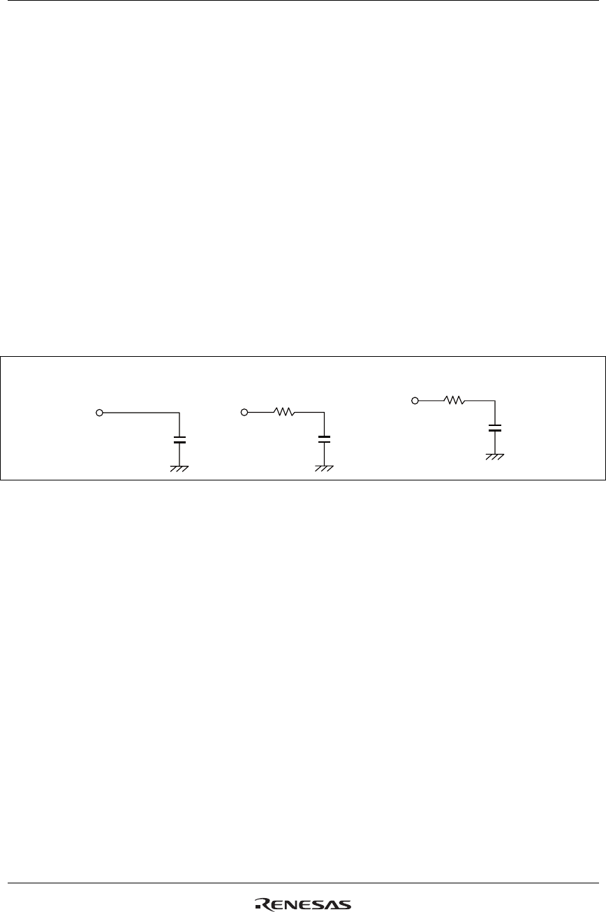
Test Circuits
<Test circuits for AC characteristics>
Test Point
Test Point
30pF
10kΩ
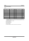
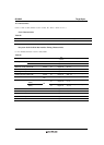
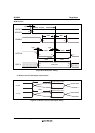
<Test circuit for VCOM output characteristics>
Test Point
10nF
[Data bus DB17-DB0]
50pF
Load capacitance C
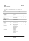
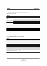
<Test circuit for LCD output characteristics>
[Liquid output: S1-S720]
Load resistance R
100Ω
Load capacitance C
Figure 78