R61509V Target Spec
Rev. 0.11 April 25, 2008, page 105 of 181
DB
17
DB
16
DB
15
DB
14
DB
13
DB
12
DB
11
DB
10
DB
9
DB
17
DB
6
DB
5
DB
14
DB
13
DB
12
DB
11
DB
10
DB
9
R5 R4 R3 R2 R1 R0 G5 G4 G3 G2 G1 G0 B5 B4 B3 B2 B1 B0
R5 R4 R3 R2 R1 R0 G5 G4 G3 G2 G1 G0 B5 B4 B3 B2 B1 B0
RD
[17]
RD
[16]
RD
[15]
RD
[14]
RD
[13]
RD
[12]
RD
[11]
RD
[10]
RD
[9]
RD
[8]
RD
[7]
RD
[6]
RD
[5]
RD
[4]
RD
[3]
RD
[2]
RD
[1]
RD
[0]
DB
17
DB
16
DB
15
DB
14
DB
13
DB
12
DB
11
DB
10
DB
9
DB
17
DB
16
DB
15
DB
14
DB
13
DB
12
DB
11
DB
10
DB
9
First transfer
Second transfer
RAM data write
RAM read data
1 pixel
GRAM data
Input
GRAM write
data
Read data
Output pins
First transfer
Second transfer
Note: Normal display in 262,144 colors.
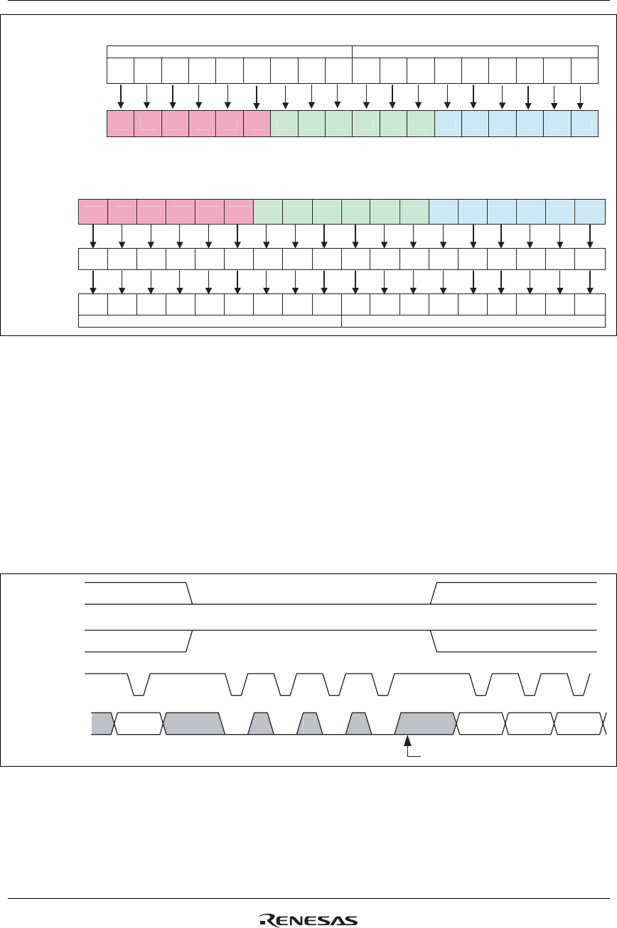
Figure 24 9-bit Interface Data Format (RAM Data Write/ RAM Data Read)
Data Transfer Synchronization in 9-bit Bus Interface Operation
The R61509V supports data transfer synchronization function to reset the counters for upper and lower 9-
bit transfers in 9-bit bus transfer mode. When a mismatch occurs in upper and lower data transfers due to
noise and so on, the 00H instruction is written four times consecutively to reset the upper and lower
counters in order to restart the data transfer from upper 9 bits. The data transfer synchronization, when
executed periodically, can help the display system recover from runaway.
Make sure to execute data transfer synchronization after reset operation before transferring instruction.
WRX
RDX
RS
(9-bit transfer synchronization)
DB17 ~ DB9
Upper
Lower
UpperUpper
Lower
"00"H "00"H "00"H "00"H
Figure 25 9-bit Data Transfer Synchronization


