R61509V Target Spec
Rev. 0.11 April 25, 2008, page 149 of 181
Power Supply Generating Circuit
The following figures show the configurations of liquid crystal drive voltage generating circuit of the
R61509V.
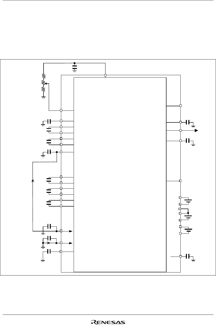
Power Supply Circuit Connection Example 1 (VCI1 = VCIOUT)
In the following example, the VCI1 level can be adjusted.
㓏⺞㔚
↢ᚑ࿁〝
VGL
DDVDH
C13M
C13P
C21M
C21P
C22M
C22P
C11M
C11P
VCI1
VCIOUT
ജ࿁〝
ౝㇱၮḰ
㔚↢ᚑ࿁〝
VCOM
ജ࿁〝
VCOMR
VREG1
ࠡࡘ࠲
VGH
࠰ࠬ
࠼ࠗࡃ
S1-720
VCOM
ࡌ࡞⺞ᢛ࿁〝
VCILVL
VDD
C12M
C12P
࿁〝㧝
࿁〝㧞
(1)
(2)
(3)
(4)
(5)
(6)
G1-432
VGH
ࠥ࠻
࠼ࠗࡃ
VGL
VCC
GND
VCI
A
GND
IOVCC
GND
VCL
VCILVL
VCOM
VCOMH
(16)
(17)
VCOML
R61509V
See note 2.
See note 1.
VREG1OUT
(7)
(8)
(9)
(10)
(11)
(15)
(12)
(13)
(14)
Figure 61
Notes: 1. The wiring resistances between the schottky diode and GND/VGL must be 5
Ω
or less.
2. The wiring resistances between the schottky diode and DDVDH/VGH must be 5
Ω
or less.


