


R61509V Target Spec
Rev. 0.11 April 25, 2008, page 93 of 181
Reset Function
The R61509V is initialized by the RESETX input. During reset period, the R61509V is in a busy state and
instruction from the microcomputer and GRAM access are not accepted. The R61509V’s internal power
supply circuit unit is initialized also by the RESETX input. The RESET period must be secured for at least
1ms. In case of power-on reset, wait until the RC oscillation frequency stabilizes (for 1 ms). During this
period, GRAM access and initial instruction setting are prohibited.
1. Initial state of instruction bits (default)
See the instruction list. The default value is shown in the parenthesis of each instruction bit cell.
2. RAM Data initialization
The RAM data is not automatically initialized by the RESETX input. It must be initialized by software in
display-off period (D1-0 = “00”).
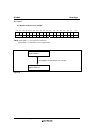
3. Output pin initial state *
see Note
1. LCD driver S1~S720 : GND
G1~G432 : VGL (= GND)
2. VCOM : Halt (GND output)
3. VCOMH : VCI
4. VCOML : Halt (GND output)
5. VREG1OUT : VGS
6. VCIOUT : Hi-z
7. DDVDH : VCI
8. VGH : DDVDH (VCI clamp)
9. VGL : GND
10. VCL : GND
11. FMARK : Halt (GND output )
12. Oscillator : Oscillate
13. SDO : High level (IOVCC1) when IM2-0 = “10*”(serial interface)
: Hi-z when IM2-0 ≠ “10*”(other than serial interface)
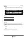
4. Initial state of input/output pins*
see Note
1. C11P : Hi-z
2. C11M : Hi-z
3. C12P : Hi-z
4. C12M : Hi-z
5. C13P : VCI1 (= Hi-z)
6. C13M : GND
7. C21P : DDVDH ( = VCI)
8. C21M : GND
9. C22P : DDVDH ( = VCI)
10. C22M : GND
11. VDD : VDD
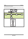
Note: The above-mentioned initial states of output and input pins are those of when the R61509V’s power
supply circuit is connected as in Connection Example.