R61509V Target Spec
Rev. 0.11 April 25, 2008, page 152 of 181
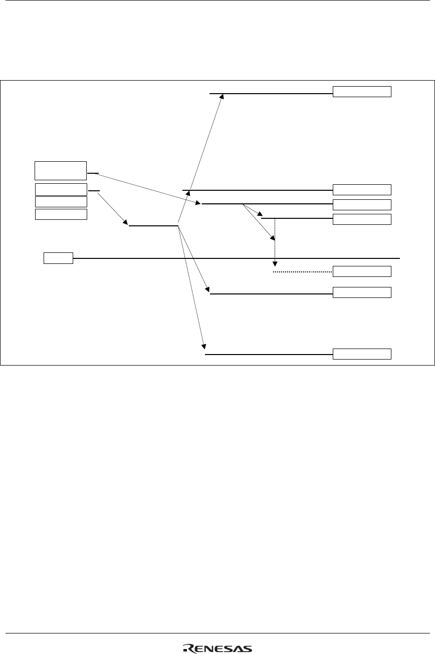
Voltage Setting Pattern Diagram
The following are the diagrams of voltage generation in the R61509V and the TFT display application
voltage waveforms and electrical potential relationship.
VGH
BT
VC
VCI1
VREG1OUT
VCM/VCOMR
VRH
VREG1OUT
DDVDH
BT
VCOML
VDV
VGL
BT
VCL
㩷
VCOMH
IOVCC(1.65~3.3V)
GND(0V)
Internal reference
voltage (VCIR)
VCC(2.5~3.3V)
VCILVL(2.5~3.3V)
Figure 63
Notes: 1. The DDVDH, VGH, VGL, and VCL output voltages will become lower than their theoretical levels
(ideal voltages) due to current consumption at each output level. Make sure that output voltage
level in operation maintains the following relationships: (DDVDH – VREG1OUT) > 0.5V, (VCOML
– VCL) > 0.5V. Also make sure VGH-VGL ≤ 28V, VCI-VCL ≤ 6V. When the alternating cycle of
VCOM is high (e.g. polarity inverts every line cycle), current consumption will increase. In this
case, check the voltage before use.
2. In operation, setting voltages within the respective voltage ranges is recommended.


