


General Information Product Description
MS278XB OM 1-3
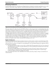
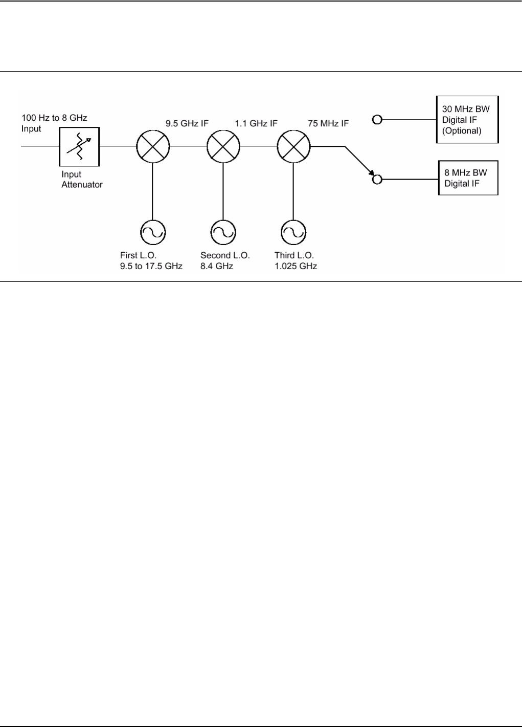
RF/Analog Architecture
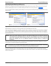
The RF/analog architecture of the Signature Signal Analyzer is designed to maximize performance over a wide
frequency and dynamic range. Signature’s basic RF/analog block diagram is shown in Figure 1-1, below:
The input signal, from either the internal 50 MHz calibrator or the test port input, is routed through the input
attenuator and then to the first mixer where it is converted to the first IF frequency of 9.5 GHz. This allows the
entire range of 100 Hz to 8 GHz to be covered in a single band without the need for preselecting. The signal is
then down-converted in the second mixer to 1.1 GHz. The frequencies of both the first and second local
oscillators can be adjusted to avoid any possible spurious response. In the third mixer, the signal is converted
to 75 MHz. While the system’s pass bandwidth up to this point has been maintained at greater than 100 MHz,
the signal path is now routed to either a wideband 75 MHz IF section, used exclusively for vector signal
analysis, or a lower bandwidth 10.7 MHz IF section, used for spectrum analysis and low bandwidth signal
analysis. While there are prefilters in the RF/analog section, the task of shaping the IF bandwidth is left
mainly to the digital section, where advanced DSP technology can be used.
Digital Architecture
The digital architecture of the Signature Signal Analyzer is built around an industry-standard Compact PCI
based embedded PC. The PC section handles all control, data management, display, and user interface aspects
of the instrument’s operation. In addition to the embedded PC, two specialized modules play important roles in
the instrument’s operation:
• The Digital IF Module employs a state-of-the-art FPGA (Field Programmable Gate Array) to perform IF
bandwidth filtering, detection, and data formatting, as well as providing the heartbeat for the real-time
data acquisition circuitry.
• The optional 30 MHz Wideband IF Module employs an advanced design analog-to-digital conversion
circuit working in conjunction with an LSI based digital signal processing section to capture large
contiguous samples of wideband I/Q data for analysis.
These two modules pass data to the embedded PC for further processing, display, storage or transmission to
external devices.
Figure 1-1. Basic Signature RF/Analog Block Diagram