


88F6281
Hardware Specifications
Doc. No. MV-S104859-U0 Rev. E Copyright © 2008 Marvell
Page 10 Document Classification: Proprietary Information December 2, 2008, Preliminary
List of Tables
1 Pin and Signal Descriptions ............................................................................................................17
Table 1: Pin Functions and Assignments Table Key ......................................................................................19
Table 2: Interface Pin Prefix Codes................................................................................................................19
Table 3: Power Pin Assignments....................................................................................................................21
Table 4: Miscellaneous Pin Assignments .......................................................................................................23
Table 5: DDR SDRAM Interface Pin Assignments .........................................................................................24
Table 6: PCI Express Interface Pin Assignments...........................................................................................26
Table 7: SATA Port Interface Pin Assignment................................................................................................27
Table 8: Gigabit Ethernet Port0/1 Interface Pin Assignments .......................................................................28
Table 9: Serial Management Interface (SMI) Pin Assignments......................................................................32
Table 10: USB 2.0 Interface Pin Assignments..................................................................................................33
Table 11: JTAG Pin Assignment.......................................................................................................................34
Table 12: RTC Interface Pin Assignments........................................................................................................35
Table 13: NAND Flash Interface Pin Assignment.............................................................................................36
Table 14: MPP Interface Pin Assignment.........................................................................................................37
Table 15: Two-Wire Serial Interface (TWSI) Interface Pin Assignment............................................................38
Table 16: UART Port 0/1 Interface Pin Assignment .........................................................................................39
Table 17: Audio (S/PDIF / I
2
S) Interface Signal Assignment............................................................................40
Table 18: Serial Peripheral Interface (SPI) Interface Signal Assignment .........................................................41
Table 19: Secure Digital Input/Output (SDIO) Interface Signal Assignment.....................................................42
Table 20: Time Division Multiplexing (TDM) Interface Signal Assignment .......................................................43
Table 21: Transport Stream (TS) Interface Signal Assignment........................................................................45
Table 22: Precise Timing Protocol (PTP) Interface Signal Assignment............................................................47
Table 23: Internal Pull-up and Pull-down Pins..................................................................................................48
2 Unused Interface Strapping.............................................................................................................49
Table 24: Unused Interface Strapping ..............................................................................................................49
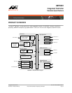
3 88F6281 Pin Map and Pin List .........................................................................................................50
4 Pin Multiplexing ................................................................................................................................51
Table 25: MPP Functionality.............................................................................................................................52
Table 26: MPP Function Summary...................................................................................................................53
Table 27: Ethernet Ports Pins Multiplexing.......................................................................................................57
Table 28: TS Port Pin Multiplexing .................................................................................................................59
5 Clocking.............................................................................................................................................60
Table 29: 88F6281Clocks.................................................................................................................................60
Table 30: Supported Clock Combinations ........................................................................................................61
6 System Power Up/Down and Reset Settings .................................................................................63
Table 31: I/O and Core Voltages......................................................................................................................63
Table 32: Reset Configuration..........................................................................................................................67