


88F6281
Hardware Specifications
Doc. No. MV-S104859-U0 Rev. E Copyright © 2008 Marvell
Page 34 Document Classification: Proprietary Information December 2, 2008, Preliminary
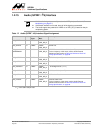
1.2.9 JTAG Interface Pin Assignment
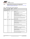
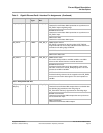
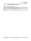
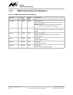
Table 11: JTAG Pin Assignment
Pin Name I/O Pin
Type
Power
Rail
Description
JT_CLK I CMOS VDDO JTAG Clock
Clock input for the JTAG controller.
NOTE: This pin is internally pulled down to 0.
JT_RSTn I CMOS VDDO JTAG Reset
When asserted, resets the JTAG controller.
NOTE: This pin is internally pulled down to 0.
1
JT_TMS_CPU I CMOS VDDO CPU JTAG Mode Select
Controls CPU JTAG controller state.
Sampled with the rising edge of JT_CLK.
NOTE: This pin is internally pulled up to 1.
JT_TMS_CORE I CMOS VDDO Core JTAG Mode Select
Controls the Core JTAG controller state.
Sampled with the rising edge of JT_CLK.
NOTE: This pin is internally pulled up to 1.
JT_TDO O CMOS VDDO JTAG Data Out
Driven on the falling edge of JT_CLK.
JT_TDI I CMOS VDDO JTAG Data In
JTAG serial data input. Sampled with the JT_CLK rising edge.
NOTE: This pin is internally pulled up to 1.
1. If this pull-down conflicts with other devices, the JTAG tool must not use this signal. This signal is not mandatory for the
JTAG interface, since the TAP (Test Access Port) can be reset by driving the JT_TMS signal HIGH for 5 JT_CLK cycles.