


Pin and Signal Descriptions
Pin Descriptions
Copyright © 2008 Marvell Doc. No. MV-S104859-U0 Rev. E
December 2, 2008, Preliminary Document Classification: Proprietary Information Page 29
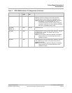
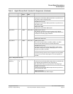
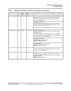
GE_RXD[3:0] I CMOS VDD_GE_A RGMII Receive Data
Contains the receive data nibble inputs that are synchronous to
GE_RXCLK input rising/falling edge.
MII/MMII Receive Data
Contains the receive data nibble inputs that are synchronous to
GE_RXCLK input.
GMII Receive Data
Contains the receive data nibble inputs.
GE_RXCTL I CMOS VDD_GE_A RGMII Receive Control
GE_RXCTL is presented on the rising edge of GE_RXCLK.
A logical derivative of receive data valid and receive data error is
presented on the falling edge of RXCLK.
MII/MMII Receive Data Valid
GMII Receive Data Valid.
GE_RXCLK I CMOS VDD_GE_A RGMII Receive Clock
The receive clock provides a 125 MHz, 25 MHz, or 2.5 MHz
reference clock derived from the received data stream.
MII/MMII Receive Clock
Provides the timing reference for the reception of the receive
data valid, receive error, and GE_RXD[3:0] signals. This clock
operates at 2.5 MHz or 25 MHz.
GMII Receive Clock
Provides the timing reference for the reception of the GE_RXDV,
receive error and receive data signals. This clock operates at
125 MHz
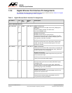
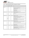
Port1—Multiplexed GbE Pins
MPP[23:20]/
GE1[3:0]
t/s
O
CMOS VDD_GE_B RGMII Transmit Data
Contains the transmit data nibble outputs that run at double data
rate with bits [3:0] presented on the rising edge of
GE_TXCLKOUT and bits [7:4] presented on the falling edge.
MII/MMII Transmit Data
Contains the transmit data nibble outputs that are synchronous
to the transmit clock input.
GMII Transmit Data
Contains the transmit data nibble outputs.
Table 8: Gigabit Ethernet Port0/1 Interface Pin Assignments (Continued)
Pin Name I/O Pin
Type
Power
Rail
Description