


88F6281
Hardware Specifications
Doc. No. MV-S104859-U0 Rev. E Copyright © 2008 Marvell
Page 24 Document Classification: Proprietary Information December 2, 2008, Preliminary
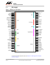
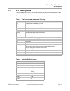
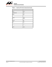
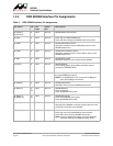
1.2.3 DDR SDRAM Interface Pin Assignments
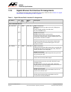
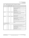
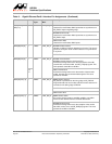
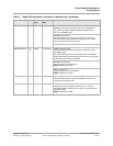
Table 5: DDR SDRAM Interface Pin Assignments
Pin Name I/O Pin
Type
Power
Rail
Description
M_CLKOUT
M_CLKOUTn
O SSTL VDD_M SDRAM Differential Clock Pair
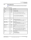
M_CKE O SSTL VDD_M Driven high to enable SDRAM clock.
Driven low when setting the SDRAM to Self-refresh mode.
M_RASn O SSTL VDD_M SDRAM Row Address Select
Asserted to indicate an active ROW address driven on the
SDRAM address lines.
M_CASn O SSTL VDD_M SDRAM Column Address Select
Asserted to indicate an active column address driven on the
SDRAM address lines.
M_WEn O SSTL VDD_M SDRAM Write Enable
Asserted to indicate a write command to the SDRAM.
M_A[14:0] O SSTL VDD_M SDRAM Address
Driven with M_BA[2:0] during RASn and CASn cycles to
generate the SDRAM address.
M_BA[2:0] O SSTL VDD_M Driven during M_RASn and M_CASn cycles to select one of
the eight SDRAM virtual banks.
NOTE: If an SDRAM device does not support the BA[2] pin,
leave the M_BA[2] unconnected.
M_CSn[3:0] O SSTL VDD_M SDRAM Chip Selects
Asserted to select a specific SDRAM Physical bank.
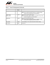
M_DQ[15:0] t/s
I/O
SSTL VDD_M SDRAM Data Bus
Driven during write.
Driven by SDRAM during reads.
M_DQS[1:0],
M_DQSn[1:0]
t/s
I/O
SSTL VDD_M SDRAM Data Strobe
Driven by the 88F6281 during write.
Driven by SDRAM during reads.
M_DM[1:0] O SSTL VDD_M SDRAM Data Mask
Asserted by the 88F6281 to select the specific byte out of the
16-bit data to be written to the SDRAM.
M_ODT[1:0] O SSTL VDD_M SDRAM On Die Termination control
Driven high to connect the SDRAM on die termination.
Driven low to disconnect the SDRAM’s termination.
NOTE: For the recommended setting, refer to the 88F6180,
88F6190, 88F6192, and 88F6281 Design Guide.