


88F6281
Hardware Specifications
Doc. No. MV-S104859-U0 Rev. E Copyright © 2008 Marvell
Page 136 Document Classification: Proprietary Information December 2, 2008, Preliminary
17. In Section 4.1, Multi-Purpose Pins Functional Summary, on page 51:
• Changed all references to MPP[0] and MPP[11] from GPI to GPIO.
• Changed the MPP[6] row in the table to remove the 0x0 option.
• Added the following bullet at the end of the section, after the tables: When TWSI serial ROM initialization is enabled,
MPP[8] and MPP[9] wake up as TWSI data and clock pins, respectively.
• Revised the description of SYSRST_OUTn.
• Added a bullet: Pin MPP[6] wakes up after reset in 0x1 mode (SYSRST_OUTn).
18. In Table 27, Ethernet Ports Pins Multiplexing, on page 57, added a new configuration option for the Gigabit Ethernet
ports: Port 0 MII/MMII, port 1 RGMII.
19. In Section 4.3, TSMP (TS Multiplexing Pins) on MPP, on page 59, added to the description of the TSMP pins.
20. Revised Table 29, 88F6281Clocks, on page 60 and Table 30, Supported Clock Combinations, on page 61.
21. Revised Section 5.1, Spread Spectrum Clock Generator (SSCG), on page 62.
22. In Section 6.2, Hardware Reset, on page 64, added
SYSRST_OUTn to the list of pins that are still active during
SYSRSTn assertion.
23. Revised Section 6.2.1, Reset Out Signal, on page 65 and Section 6.2.3, SYSRSTn Duration Counter, on page 65 and
added Section 6.2.2, Power On Reset (POR), on page 65.
24. In Section 6.3.2, PCI Express Endpoint Reset, on page 66 revised the bulleted items.
25. Revised Section 6.5, Pins Sample Configuration, on page 66.
26. Made major revisions to Table 32, Reset Configuration, on page 67.
27. Revised the first two paragraphs in Section 6.6, Serial ROM Initialization, on page 70.
28. In Section 6.7, Boot Sequence, on page 71 revised the paragraph following step 4.
29. Revised Table 45, Reference Clock AC Timing Specifications, on page 86.
30. In Table 34, IDCODE Register Map, on page 74, revised the description of bits [31:28].
31. In Table 35, Absolute Maximum Ratings, on page 75:
• Added VHV.
• Revised the voltage for the SATA and XTAL AVDD parameters.
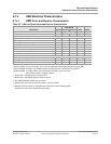
32. In the Table 36, Recommended Operating Conditions, on page 77:
• Added values for VDD_CPU.
• Added VHV and revised the voltage for the SATA and XTAL AVDD parameters.
• For the 3.3V interfaces, revised the minimum value to 3.15V and the maximum value to 3.45V (+/-5%).
• Revised the description of the VDD_GE_A/VDD_GE_B row, to show that RGMII can also operate with a voltage of
3.3V.
• Revised the values for PEX_AVDD to minimum 1.7V, typical 1.8V, and maximum 1.9V.
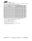
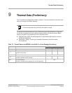
33. In Table 37, Thermal Power Dissipation, on page 79
• Revised values for Core, Embedded CPU, PCI Express, USB and SATA parameters.
• Changed all occurrences of VDD_CPU to VDD.
• Added the row RGMII 3.3V interface.
• Revised the notes following the table, to remove reference to the trace length or resistance.
34. In Table 38, Current Consumption, on page 80
• Revised values for Core, Embedded CPU, SATA, PCI Express and USB parameters.
• Changed all occurrences of VDD_CPU to VDD.
• Revised the interface RGMII 1.8V interface to RGMII 1.8V or 3.3V interface.
• Revised the notes following the table to remove reference to the trace length or resistance.
35. Deleted Section 8.5.2 REF_CLK_XIN 2.5V (CMOS) DC Electrical Specifications and added pin REF_CLK_XIN to
Section 8.5.2, RGMII, SMI and REF_CLK_XIN 1.8V (CMOS) DC Electrical Specifications, on page 82, since the
power rail for the REF_CLK_XIN pin was changed from 2.5V to 1.8V.
36. In Section 8.5.1, General 3.3V (CMOS) DC Electrical Specifications, on page 81, added reference to PTP and RGMII.
37. Revised Table 64, PCI Express Interface Differential Reference Clock Characteristics, on page 118 and Table 65, PCI
Express Interface Spread Spectrum Requirements, on page 119.
Table 75: Revision History (Continued)
Revision Date Comments