Pin and Signal Descriptions
Pin Descriptions
Copyright © 2008 Marvell Doc. No. MV-S104859-U0 Rev. E
December 2, 2008, Preliminary Document Classification: Proprietary Information Page 23
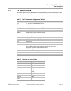
1.2.2 Miscellaneous Pin Assignment
The Miscellaneous signal list contains clock and reset, test, and related signals.
Table 4: Miscellaneous Pin Assignments
Pin Name I/O Pin
Type
Power
Rail
Description
REF_CLK_XIN I Analog XTAL_AVDD Reference clock input from external oscillator or input from
external crystal. Used as input to core, CPU, SATA, and USB
PLLs.
XOUT O Analog XTAL_AVDD XTAL_OUT
Feedback signal to external crystal.
When not used, leave this pin floating.
SYSRSTn I CMOS VDDO System reset
Main reset signal of the device clock. Used to reset all units
to their initial state.
When in the reset state, most output pins are in Tri-State.
SYSRST_OUTn O CMOS VDDO Reset request from the device to the board reset logic.
This pin is multiplexed on the MPP pins (see Section 4, Pin
Multiplexing, on page 51).
PEX_RST_OUTn O CMOS VDDO Optional PCI Express Endpoint card reset output
This pin is multiplexed on the MPP pins (see Section 4, Pin
Multiplexing, on page 51).
TP O Analog Analog Test Point for SATA, USB, and PCI Express
interfaces
For internal use. Leave this pin unconnected.
ISET I Analog Current reference for both the USB and SATA PHYs.
Terminate this pin with a 6.04 k
Ω resistor, pulled down.
MRn I CMOS VDD_GE_A Active-Low, Manual Reset Input
SYSRST_OUTn is asserted low as long as the MRn input
signal is asserted low, and for additional 20 ms after MRn
(manual reset) de-assertion
This pin is internally pulled up.
RESERVED Reserved for Marvell
®
future usage.
Leave unconnected externally.
NC Reserved for Marvell
®
future usage.
Leave unconnected externally.


