


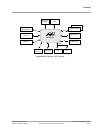

88F6281
Hardware Specifications
Doc. No. MV-S104859-U0 Rev. E Copyright © 2008 Marvell
Page 8 Document Classification: Proprietary Information December 2, 2008, Preliminary
Table of Contents
Product Overview.......................................................................................................................................3
Features.......................................................................................................................................................4
Preface.......................................................................................................................................................15
About this Document.......................................................................................................................................15
Related Documentation...................................................................................................................................15
Document Conventions...................................................................................................................................16
1 Pin and Signal Descriptions.......................................................................................................17
1.1 Pin Logic .........................................................................................................................................................18
1.2 Pin Descriptions ..............................................................................................................................................19
1.3 Internal Pull-up and Pull-down Pins ................................................................................................................48
2 Unused Interface Strapping........................................................................................................49
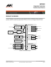
3 88F6281 Pin Map and Pin List ....................................................................................................50
4 Pin Multiplexing...........................................................................................................................51
4.1 Multi-Purpose Pins Functional Summary........................................................................................................51
4.2 Gigabit Ethernet (GbE) Pins Multiplexing on MPP..........................................................................................57
4.3 TSMP (TS Multiplexing Pins) on MPP.............................................................................................................59
5 Clocking .......................................................................................................................................60
5.1 Spread Spectrum Clock Generator (SSCG)....................................................................................................62
6 System Power Up/Down and Reset Settings............................................................................63
6.1 Power-Up/Down Sequence Requirements......................................................................................................63
6.2 Hardware Reset ..............................................................................................................................................64
6.3 PCI Express Reset..........................................................................................................................................66
6.4 Sheeva
™
CPU TAP Controller Reset..............................................................................................................66
6.5 Pins Sample Configuration..............................................................................................................................66
6.6 Serial ROM Initialization..................................................................................................................................70
6.7 Boot Sequence................................................................................................................................................71
7 JTAG Interface.............................................................................................................................73
7.1 TAP Controller.................................................................................................................................................73
7.2 Instruction Register .........................................................................................................................................73
7.3 Bypass Register..............................................................................................................................................74
7.4 JTAG Scan Chain ...........................................................................................................................................74
7.5 ID Register ......................................................................................................................................................74