Pin and Signal Descriptions
Pin Descriptions
Copyright © 2008 Marvell Doc. No. MV-S104859-U0 Rev. E
December 2, 2008, Preliminary Document Classification: Proprietary Information Page 19
1.2 Pin Descriptions
This section details all the pins for the different interfaces providing a functional description of each
pin and pin attributes.
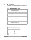
Table 1<Default ¬¹ Font> defines the abbreviations and acronyms used in the pin description tables.
Table 1: Pin Functions and Assignments Table Key
Term Definition
[n] n - Represents the SERDES pair number
<n> Represents port number when there are more than one ports
Analog Analog Driver/Receiver or Power Supply
Calib Calibration pad type
CML Common Mode Logic
CMOS Complementary Metal-Oxide-Semiconductor
DDR Double Data Rate
GND Ground Supply
HCSL High-speed Current Steering Logic
I Input
I/O Input/Output
O Output
o/d Open Drain pin
The pin allows multiple drivers simultaneously (wire-OR connection).
A pull-up is required to sustain the inactive value.
Power VDD Power Supply
SSTL Stub Series Terminated Logic for 1.8V
t/s Tri-State pin
XXXn n - Suffix represents an Active Low Signal
Table 2: Interface Pin Prefix Codes
Interface Prefix
Misc N/A
DDR SDRAM M_
PCI Express PEX_
SATA SATA0_
SATA1_
Gigabit Ethernet GE_
USB 2.0 USB_
JTAG JT_


