Revision History
Copyright © 2008 Marvell Doc. No. MV-S104859-U0 Rev. E
December 2, 2008, Preliminary Document Classification: Proprietary Information Page 135
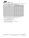
17. In Table 36, Recommended Operating Conditions, on page 77:
• For VHV, revised the two parameters to VHV (during eFuse Burning mode) and VHV (during eFuse Reading mode)
and added notes in the comments column for both VHV voltages.
• For VDD_M, PEX_AVDD, and USB_AVDD, revised the comments column.
• for RTC_AVDD, revised the values for minimum to 1.4V from 1.3V and for maximum to 1.6V from 1.7V.
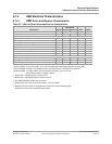
18. In Table 37, Thermal Power Dissipation, on page 79, revised the row for the SDRAM and added a row for the eFuse.
19. In Table 38, Current Consumption, on page 80, revised the row for the SDRAM and added a row for the eFuse.
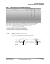
20. In Table 45, Reference Clock AC Timing Specifications, on page 86:
• For the CPU and Core Reference Clock frequency, revised the values.
• For the PTP Reference Clock, added the Slew rate and Pk-Pk jitter parameters.
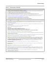
C August 18, 2008 Revision
1. Added the XOR engine to the block diagram in the Product Overview on page 3.
2. Added AN-249: Configuring the Marvell® SATA PHY to Transmit Predefined Test Patterns to the list of Related
Documentation on page 15.
3. In Figure 1, 88F6281 Pin Logic Diagram, on page 18, added VHV, and MRn and changed PEX_CLK_P/N for input to
input/output (I/O).
4. In the pin map and pin list, revised pins F04 to MRn and G04 to VHV.
5. In Table 3, Power Pin Assignments, on page 21:
• Added VHV.
• Changed the voltage for XTAL_AVDD from 2.5V to 1.8V.
• Changed the voltage for SATA0_AVDD/SATA1_AVDD from 2.5V to 3.3V.
• Revised the description of VDD_GE_A and VDD_GE_B to add additional information about RGMII.
6. In Table 4, Miscellaneous Pin Assignments, on page 23, added the signal MRn.
7. In Table 5, DDR SDRAM Interface Pin Assignments, on page 24, revised the description of M_NCASL and M_PCAL to
indicate the range of the resistor.
8. In Table 6, PCI Express Interface Pin Assignments, on page 26, changed PEX_CLK_P/N for input to input/output (I/O).
9. Added present and active pins to Table 7, SATA Port Interface Pin Assignment, on page 27.
10. In Section 1.2.6, Gigabit Ethernet Port Interface Pin Assignments, on page 28:
• Added a note: For the TXCLK, use the GE_RXCLK pin. Also indicated which pins are for port0 and which for port1.
•In Table 8, Gigabit Ethernet Port0/1 Interface Pin Assignments, on page 28, added a description for MII/MMII to the
GE_TXD[3:0], GE_TXCTL, GE_RXCTL, GE_RXCLK, GE_RXD[3:0] rows. Also for pin MPP[30]/GE1[10] added a
description for MII/MMII Receive Data Valid.
11. In Table 17, Audio (S/PDIF / I
2
S) Interface Signal Assignment, on page 40, revised the power rail to
VDDO/VDD_GE_B.
12. Revised Table 19, Secure Digital Input/Output (SDIO) Interface Signal Assignment, on page 42 to indicate the pins
requiring pull up.
13. Added Table 21, Transport Stream (TS) Interface Signal Assignment, on page 45.
14. Added Section 1.2.20, Precise Timing Protocol (PTP) Interface, on page 47.
15. In Table 23, Internal Pull-up and Pull-down Pins, on page 48, revised the pin numbers and changed pins GE_MDC,
MPP[7] and MPP[18] from pull down to pull up and removed MPP[13], MPP[15], and MPP[17] from the table, since
they do not require a pull up/down.
16. In Table 2, Unused Interface Strapping, on page 49, revised the description of the strapping for the
SATA0_AVDD/SATA1_AVDD pins.
Table 75: Revision History (Continued)
Revision Date Comments


