


88F6281
Hardware Specifications
Doc. No. MV-S104859-U0 Rev. E Copyright © 2008 Marvell
Page 134 Document Classification: Proprietary Information December 2, 2008, Preliminary
A Revision History
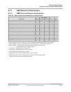
Table 75: Revision History
Revision Date Comments
E December 2, 2008
Revision
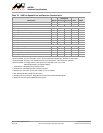
1. In Figure
1, 88F6281 Pin Logic Diagram, on page 18, changed the GE_TXCLKOUT pin to input/output and added a
note under the figure, stating that the pin is an input when used the MII/MMII Transmit Clock.
2. In Table 6, PCI Express Interface Pin Assignments, on page 26, revised the description of the PEX_CLK_P/N pins to
state that they can be configured as input or output according to the reset strap.
3. In Table 8, Gigabit Ethernet Port0/1 Interface Pin Assignments, on page 28, indicated that:
• When the GE_TXCLKOUT pin is used as an MII/MMII Transmit Clock, it is an input pin.
• When the MPP[29]/GE1[9] pin is used as a GMII Transmit Clock, it is a Tri-State output pin.
4. In Table 12, RTC Interface Pin Assignments, on page 35, changed the type for RTC_XOUT to analog.
5. In the description of signal AU_SPDFRMCLK in Table 17, Audio (S/PDIF / I
2
S) Interface Signal Assignment, on
page 40, added a reference to the new AU_SPDFRMCLK information in the Reference Clock AC Timing
Specifications table.
6. In Table 24, Unused Interface Strapping, on page 49
, revise the description for configuring the PCI Express clock
signals.
7. At the end of Section 4.2, Gigabit Ethernet (GbE) Pins Multiplexing on MPP, on page 57, added a note stating that all
relevant Gigabit Ethernet signals must be implemented.
8. In the Table 32, Reset Configuration, on page 67, revised the configuration function for parameter CPU_CLK to DDR
CLK Ratio.
9. In Table 36, Recommended Operating Conditions, on page 77, for parameter RTC_AVDD Analog supply for RTC in
Battery Back-up mode, revised the values for the minimum to 1.3V from 1.4V and for the maximum to 1.7V from 1.6V.
10. In Table 37, Thermal Power Dissipation, on page 79:
• For the Embedded CPU (VDD_CPU 1.1V) parameter changed the L2 cache frequency to 333 MHz.
• for the eFuse during Burning mode parameter added a note:
The eFuse burn is done once, and there should be no thermal effect, after it has been burned.
11. In Table 38, Current Consumption, on page 80, for the Embedded CPU (VDD_CPU 1.1V) parameter changed the L2
cache frequency to 333 MHz.
12. In Table 45, Reference Clock AC Timing Specifications, on page 86:
• Revised the names of the Ethernet transmit symbols to F
GE_TXCLK_OUT
,
DC
GE_TXCLK_OUT
, and SR
GE_TXCLK_OUT
.
• Added the S/PDIF Recovered Master Clock.
• Added the Transport Stream External Reference Clock.
• For the PTP Reference Clock, revised the values for the Frequency, Duty Cycle, and Pk-Pk jitter parameters.
13. In Table 46, SDRAM DDR2 Interface AC Timing Table, on page 88, revised the minimum value for symbol tDHI to 0.70
ns from 0.72 ns.
D October 5, 2008 Revision
14. In Table 6, PCI Express Interface Pin Assignments, on page 26, revised the note in the description of the
PEX_CLK_P/N pins.
15. In Table 24, Unused Interface Strapping, on page 49, added the eFuse strapping.
16. In Section 6.1.1, Power-Up Sequence Requirements, on page 63 and Section 6.1.2, Power-Down Sequence
Requirements, on page 64, added a power up/down requirements for when VHV is in eFuse Burning mode.