


Pin and Signal Descriptions
Pin Descriptions
Copyright © 2008 Marvell Doc. No. MV-S104859-U0 Rev. E
December 2, 2008, Preliminary Document Classification: Proprietary Information Page 43
1.2.18 Time Division Multiplexing (TDM) Interface
Note
All of the TDM signals are multiplexed on the MPP pins (see Section 4, Pin
Multiplexing, on page 51).
The TDM signals are powered on VDDO or on VDD_GE_B, based on the pin
multiplexing option (see Section 4, Pin Multiplexing, on page 51).
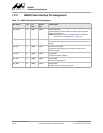
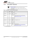
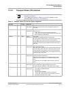
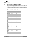
Table 20: Time Division Multiplexing (TDM) Interface Signal Assignment
Pin Name
I/O
Pin Type Power Rail
Description
TDM_CH0_TX_
QL
O CMOS VDDO/
VDD_GE_B
TDM Channel0 Transmit Qualifier
TDM_CH2_TX_
QL
O CMOS VDDO/
VDD_GE_B
TDM Channel2 Transmit Qualifier
TDM_CH0_RX_
QL
O CMOS VDDO/
VDD_GE_B
TDM Channel0 Receive Qualifier
TDM_CH2_RX_
QL
O CMOS VDDO/
VDD_GE_B
TDM Channel2 Receive Qualifier
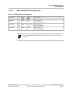
TDM_CODEC_
INTn
I CMOS VDDO/
VDD_GE_B
Interrupt Signal FROM the SLIC/codec
TDM_CODEC_
RSTn
O CMOS VDDO/
VDD_GE_B
SLIC/codec
Reset Signal
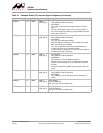
TDM_PCLK I/O CMOS VDDO/
VDD_GE_B
PCM Audio Bit Clock
TDM_FS I/O CMOS VDDO/
VDD_GE_B
TDM Frame Sync Signal
TDM_DRX I CMOS VDDO/
VDD_GE_B
PCM Audio Input Data (for recording)
TDM_DTX O CMOS VDDO/
VDD_GE_B
PCM Audio Output Data (for playback)
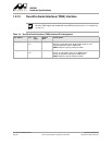
TDM_SPI_CS[1:0]
O CMOS VDDO/
VDD_GE_B
Active low SPI chip selects driven by the host to the codec for
register access. Always asserted for eight SCLK cycles at a time.
Only Byte-by-Byte mode codec register read/write is supported.
TDM_SPI_SCK O CMOS VDDO/
VDD_GE_B
Serial SPI clock from the host to the codec for register access.
This is an RTO (return to one) clock. It toggles for eight cycles at
a time (for 1 byte transfer) during codec register access, then it
returns to high.
The host drives write data on TDM_SPI_MOSI on the negative
edge of TDM_SPI_SCK, and captures read data from the codec
on the positive edge of TDM_SPI_SCK.