


88F6281
Hardware Specifications
Doc. No. MV-S104859-U0 Rev. E Copyright © 2008 Marvell
Page 30 Document Classification: Proprietary Information December 2, 2008, Preliminary
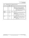
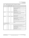
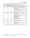
MPP[27:24]/
GE1[7:4]
I CMOS VDD_GE_B RGMII Receive Data
Contains the receive data nibble inputs that are synchronous to
GE_RXCLK input rising/falling edge.
MII/MMII Receive Data
Contains the receive data nibble inputs that are synchronous to
GE_RXCLK input.
GMII Receive Data
Contains the receive data nibble inputs.
MPP[28]/GE1[8] I CMOS VDD_GE_B MII/MMII Collision Detect
Indicates a collision has been detected on the wire. This input is
ignored in full-duplex mode. Collision detect is not synchronous
to any clock.
GMII Collision Detect
MPP[29]/GE1[9] I CMOS VDD_GE_B MII/MMII Transmit Clock
MII/MMII transmit reference clock from PHY.
Provides the timing reference for the transmission of the MII
transmit clock, transmit enable, and GE_TXD[3:0] signals. This
clock operates at 2.5 MHz or 25 MHz.
t/s
O
GMII Transmit Clock
Provides the timing reference for the transfer of the transmit
enable, transmit error and transmit data signals. This clock
operates at 125 MHz.
MPP[30]/GE1[10] I CMOS VDD_GE_B RGMII Receive Control
GE_RXCTL is presented on the rising edge of GE_RXCLK.
A logical derivative of receive data valid and receive data error is
presented on the falling edge of RXCLK.
MII/MMII Receive Data Valid
GMII Receive Error
MPP[31]/GE1[11] I CMOS VDD_GE_B RGMII Receive Clock
The receive clock provides a 125 MHz, 25 MHz, or 2.5 MHz
reference clock derived from the received data stream.
MII/MMII Receive Clock
Provides the timing reference for the reception of the receive
data valid, receive error, and GE_RXD[3:0] signals. This clock
operates at 2.5 MHz or 25 MHz.
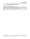
Table 8: Gigabit Ethernet Port0/1 Interface Pin Assignments (Continued)
Pin Name I/O Pin
Type
Power
Rail
Description