88F6281
Hardware Specifications
Doc. No. MV-S104859-U0 Rev. E Copyright © 2008 Marvell
Page 56 Document Classification: Proprietary Information December 2, 2008, Preliminary
Note
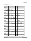
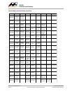
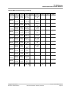
For MPPs assigned as NAND flash and SPI flash, wake-up mode after reset
depends on Boot mode (see the Boot Device field in Table 32, Reset
Configuration, on page 67):
• When Boot mode is NAND Flash, MPP[5:0] and MPP[19:18] wake up after reset
in NAND Flash mode.
• When Boot mode is SPI Flash, either MPP[3:0] or {MPP[3:1] and MPP[7]} wake
up after reset in SPI mode, (according to boot mode configured by reset strap
pins).
Pin MPP[6] wakes up after reset in 0x1 mode (SYSRST_OUTn)
Pin MPP[7] wakes up after reset:
• As SPI_CSn, if the boot device—selected according to boot device reset
strapping—is 0x2 (boot from SPI flash, SPI_CSn on MPP[7]).
• As PEX_RST_OUTn, if the boot device—selected according to boot device
reset strapping—is any option other than 0x2.
When TWSI serial ROM initialization is enabled (see TWSI Serial ROM
Initialization in Table 32, Reset Configuration, on page 67), MPP[8] and MPP[9]
wake up as TWSI data and clock pins, respectively.
All other MPP interface pins wake up after reset in 0x0 mode (GPIO/GPO) and are
default set to Data Output disabled (Tri-State). Therefore, those MPPs that are
GPIO are in fact inputs, and those that are GPO are Tri-State.
The SPI interface can be configured using one of the following sets of MPP pins:
• MPP[3:0]
• MPP[11], MPP[10], MPP[7], and MPP[6]
• MPP[3:1] and MPP[7]
Do not configure both MPP[3] and MPP[11] as SPI_MISO.
UART0 and UART1 signals are duplicated on a few MPPs. The UART0 or UART1
signals must not be configured to more than one MPP.
When selecting the MII/MMII interface (MPP[35:20]) and the TDM interface
(MPP[49:35]), the TDM signal TDM_CH0_TX_QL and the MII/MMII signal
MII1_RXERR are both multiplexed on MPP[35]. However, MPP[35] can only be
configured to one of these functions at a time.
Some of the MPP pins are sampled during SYSRSTn de-assertion to set the
device configuration. These pins must be set to the correct value during reset (see
Section 6.5, Pins Sample Configuration, on page 66).
Pins that are left as GPIO and are not connected should be set to output after
SYSRSTn de-assertion.


