Pin and Signal Descriptions
Pin Descriptions
Copyright © 2008 Marvell Doc. No. MV-S104859-U0 Rev. E
December 2, 2008, Preliminary Document Classification: Proprietary Information Page 45
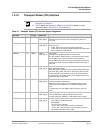
1.2.19 Transport Stream (TS) Interface
Note
All of the TS signals are multiplexed on the MPP pins (see Section 4, Pin
Multiplexing, on page 51).
The TS signals are powered on VDDO or on VDD_GE_B based on the pin
multiplexing option (see Section 4, Pin Multiplexing ).
Table 21: Transport Stream (TS) Interface Signal Assignment
Pin Name
I/O
Pin Type Power Rail
Description
TSMP[0] I CMOS VDDO/
VDD_GE_B
EXT_CLK
External clock that can be used to drive the TS0_CLK and
TS1_CLK
TSMP[1] I/O CMOS VDDO/
VDD_GE_B
TS0_CLK
Port0 TS clock.
• If TS0_VAL is used, the clock may be continuous.
• If TS0_VAL is not used, the clock may toggle only when valid
data is available on TS0_DATA.
TSMP[2] I/O CMOS VDDO/
VDD_GE_B
TS0_SYNC
Port0 Sync/Frame Start Indicator or Packet Clock.
The TS0_SYNC in parallel mode is a pulse that is active during
the first (Sync) byte of the TS packet. In serial mode, the
TS0_SYNC pulse may be active for the entire byte or only for the
first bit. The polarity is programmable to be either active high or
active low.
TSMP[3] I/O CMOS VDDO/
VDD_GE_B
TS0_VAL
Port0 Valid Data Indicator
When this signal is used and is valid, it indicates that valid data is
present on TS0_DATA. TS0_VAL is active during the TS frame
packet data and inactive when there is no TS synchronization.
In output mode, the polarity of TS0_VAL is programmable to be
either active high or active low.
TSMP[4] I/O CMOS VDDO/
VDD_GE_B
TS0_ERR
Port0 Uncorrectable Packet Error
When this signal is used, an error indicates that the packet
contains an uncorrectable error, and therefore should not be
used.
In output mode, the TS0_ERR is active during the entire TS
frame.
TSMP[5] I/O CMOS VDDO/
VDD_GE_B
TS0_DATA[0]
Port0 TS Data bit 0 in both parallel and serial modes.
In Serial mode TS0_DATA[0] is used as data input or output.
TSMP[6] I/O CMOS VDDO/
VDD_GE_B
• Parallel Mode:
TS0_DATA[1]: Port0 TS Data bit 1
• Serial Mode:
TS1_CLK: Port1 TS clock.
- If TS1_VAL is used, the clock may be continuous.
- If TS1_VAL is not used, the clock may toggle only when
valid data is available on TS1_DATA


