


Revision History
Copyright © 2008 Marvell Doc. No. MV-S104859-U0 Rev. E
December 2, 2008, Preliminary Document Classification: Proprietary Information Page 137
38. Revised Figure 25, TWSI Output Delay AC Timing Diagram, on page 104 so that it shows SDA t
OV
relative to the SCK
falling edge, as shown in the two tables that proceed the figure.
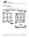
39. In Table 73, HSBGA 288-pin Package Dimensions, on page 131, changed the maximum value for the parameter H/S
exposed size to 13.200 mm.
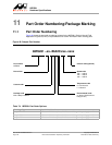
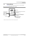
40. Revised all of Section 11, Part Order Numbering/Package Marking, on page 132.
B April 8, 2008 Revision
1. In the features list:
• Added the bullets Precise Timing Protocol (PTP) and Audio Video Bridging networks.
• Added the functional block diagram and the usage model diagram.
2. Throughout this specification, LVCMOS and LVTTL were changed to CMOS.
3. In Figure 1, 88F6281 Pin Logic Diagram, on page 18 revised the power pins and removed the interfaces that are
multiplexed on the MPP pins.
4. Revised Table 1, Pin Functions and Assignments Table Key, on page 19 to show only terms relevant for this device.
5. In Table 3, Power Pin Assignments, on page 21, added pins SSCG_AVDD and SSCG_AVSS and added the SMI
interface at 1.8V and the MII/MMII interface at 3.3V to the description of the interfaces supported by pin VDD_GE_A.
6. In Table 8, Gigabit Ethernet Port0/1 Interface Pin Assignments, on page 28, removed pins GE_MDC and GE_MDIO.
7. Added Section 1.2.7, Serial Management Interface (SMI) Interface Pin Assignments, on page 32, with a description of
the GE_MDC and GE_MDIO pins.
8. In Table 12, RTC Interface Pin Assignments, on page 35, changed the pin type for RTC_XIN to analog from CMOS.
9. In Table 15, Two-Wire Serial Interface (TWSI) Interface Pin Assignment, on page 38, changed the note to:
Requires a pull-up resistor to VDDO.
10. Added Section 2, Unused Interface Strapping, on page 49.
11. In Table 29, 88F6281Clocks, on page 60, revised the description of CPU PLL to mention SSCG.
12. Added Section 5.1, Spread Spectrum Clock Generator (SSCG), on page 62.
13. Added Section 6.1, Power-Up/Down Sequence Requirements, on page 63 and revised the title of Section 6 to reflect
this change.
14. In Section 6.4, Sheeva
™
CPU TAP Controller Reset, on page 66, revised the note referring to sample at reset and
added the note: If a signal is pulled up on the board, it must be pulled to the proper voltage level. Certain reset
configuration pins are powered by VDD_GE_A and VDD_GE_B. Those pins have multiple voltage options (see
Table 36, Recommended Operating Conditions, on page 77).
15. In Table 35, Absolute Maximum Ratings, on page 75 and Table 36, Recommended Operating Conditions, on page 77,
added the parameter SSCG_VDD.
16. In Table 37, Thermal Power Dissipation, on page 79 added the following:
The purpose of the Thermal Power Dissipation table is to support system engineering in thermal design.
17. In Table 38, Current Consumption, on page 80 added the following:
The purpose of the Current Consumption table is to support board power design and power module selection.
18. In Table 45, Reference Clock AC Timing Specifications, on page 86:
• Revised the symbols for the Transport Stream (TS) output and input mode reference clocks.
• Revised the symbols for the SMI master mode reference clock.
• Revised the symbols for the TWSI master mode reference clock.
• Revised the description for symbol F
RTC_XIN.
• Removed the RGMII, GMII, MII 100 Mbps, and MII 10 Mbps rows, since they are not relevant to this device.
19. In Table 67, SATA-I Interface Gen1i Mode Driver and Receiver Characteristics, on page 123, added driver and
receiver return loss parameters, according to updated standard.
A January 28, 2008 Initial release
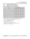
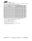
Table 75: Revision History (Continued)
Revision Date Comments