


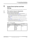
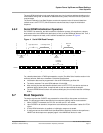

System Power Up/Down and Reset Settings
Pins Sample Configuration
Copyright © 2008 Marvell Doc. No. MV-S104859-U0 Rev. E
December 2, 2008, Preliminary Document Classification: Proprietary Information Page 67
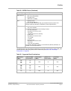
In each row of Table 32, the order of the pins is from MSb to LSb (e.g., for in the row CPU_CLK
Frequency Select, MPP[2] is the MSB and MPP[10] is the LSB).
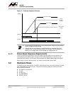
Note
If external logic is used instead of pull-up and pull-down resistors, the logic must
drive all of these signals to the desired values during SYSRSTn assertion. To
prevent bus contention on these pins, the external logic must float the bus no later
than the third TCLK cycle after SYSRSTn de-assertion.
All reset sampled values are registered in the Sample at Reset register (see the
MPP Registers in the 88F6180, 88F6190, 88F6192, and 88F6281 Functional
Specifications). This is useful for board debug purposes and identification of board
and system settings for the host software.
If a signal is pulled up on the board, it must be pulled to the proper voltage level.
Certain reset configuration pins are powered by VDD_GE_A and VDD_GE_B.
Those pins have multiple voltage options (see Table 36, Recommended Operating
Conditions, on page 77).
Table 32: Reset Configuration
Pin Configuration Function
MPP[1] TWSI Serial ROM Initialization
0 = Disabled
1 = Enabled
NOTE: Internally pulled down to 0x0.
When this pin is set to 0x1, MPP[8] and MPP[9] wake up as TWSI data and clock pins,
respectively (see Section 4.1, Multi-Purpose Pins Functional Summary, on page 51).
MPP[2],MPP[5],
MPP[19],
MPP[10]
CPU_CLK Frequency Select
0x0–0x6 = Reserved
0x7 = 1000 MHz
0x8 = Reserved
0x9 = 1200 MHz
0xA–0xB = Reserved
0xC = 1500 MHz
0xD–0xF = Reserved
NOTE: Internally pulled to 0x6.
The supported combination for CPU_CLK Frequency select, CPU_CLK to DDR CLK ratio,
and CPU_CLK to CPU L2 clock ratio are listed in Table 30, Supported Clock Combinations,
on page 61.