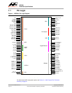
Pin and Signal Descriptions
Pin Descriptions
Copyright © 2008 Marvell Doc. No. MV-S104859-U0 Rev. E
December 2, 2008, Preliminary Document Classification: Proprietary Information Page 21
1.2.1 Power Supply Pins
Table 3 provides the voltage levels for the various interface pins. These do not include the analog
power supplies for the PLLs or PHYs which are explicitly mentioned in the other pin description
tables.
Table 3: Power Pin Assignments
Pin Name I/O Pin
Type
Description
VDD I Power 1.0V Digital core voltage
VDD_CPU I Power 1.1V Digital CPU voltage
VDDO I Power 3.3V I/O power for MPP[49:36],MPP[19:0] and JTAG pins
VDD_GE_A I Power 1.8V or 3.3V I/O supply voltage for RGMII and SMI interfaces
3.3V I/O supply voltage for GMII, MII/MMII, and SMI interfaces
VDD_GE_B I Power I/O power for MPP[35:20]
1.8V or 3.3V I/O supply voltage for RGMII interfaces
3.3V I/O supply voltage for GMII and MII/MMII interfaces
VDD_M I Power 1.8V I/O supply voltage for the DDR2 SDRAM interface
VSS I GND VSS
CPU_PLL_AVDD I Power 1.8V analog quiet power to CPU PLL
NOTE: See the 88F6180, 88F6190, 88F6192, and 88F6281 Design
Guide
for power supply filtering recommendations.
CPU_PLL_AVSS I GND CPU PLL ground
CORE_PLL_AVDD I Power 1.8V analog quiet power to Core PLL
NOTE: See the 88F6180, 88F6190, 88F6192, and 88F6281 Design
Guide for power supply filtering recommendations.
CORE_PLL_AVSS I GND Core PLL ground
SSCG_AVDD I Power 1.8V quiet power supply to the internal Spread Spectrum Clock
Generator
SSCG_AVSS I GND Ground for the internal Spread Spectrum Clock Generator
XTAL_AVDD I Power 1.8V analog quiet power to on-chip clock inverter for supporting external
crystal, and on-chip current reference for SATA and USB PHYs
NOTE: See the 88F6180, 88F6190, 88F6192, and 88F6281 Design
Guide for power supply filtering recommendations.
XTAL_AVSS I GND Ground for supporting external crystal, and on-chip current reference for
SATA and USB PHYs
VHV I Power I/O supply voltage for eFuse:
• 2.5V for eFuse burning only
• 1.0V for eFuse reading only


