Electrical Specifications
AC Electrical Specifications
Copyright © 2008 Marvell Doc. No. MV-S104859-U0 Rev. E
December 2, 2008, Preliminary Document Classification: Proprietary Information Page 109
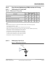
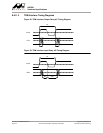
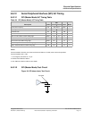
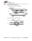
8.6.11 Time Division Multiplexing (TDM) Interface AC Timing
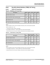
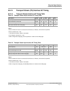
8.6.11.1 TDM Interface AC Timing Table
Table 59: TDM Interface AC Timing Table
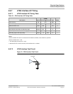
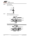
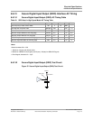
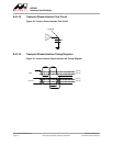
8.6.11.2 TDM Interface Test Circuit
Figure 31: TDM Interface Test Circuit
Min Max
PCLK cycle time 1/tC 0.256 8.192 MHz 1, 3
PCLK duty cycle tDTY 0.4 0.6 tC 1
PCLK rise/fall time tR/tF - 3.0 ns 1, 2, 8
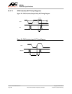
DTX and FSYNC valid after PCLK rising edge tD 0.0 20.0 ns 1, 4, 6
DRX and FSYNC setup time relative to PCLK falling edge tSU 10.0 - ns 5, 7
DRX and FSYNC hold time relative to PCLK falling edge tHD 10.0 - ns 5, 7
Note s:
General comment: All values were measured from vddio/2 to vddio/2, unless otherw ise specified.
1. For all signals, the load is CL = 20 pF.
2. Rise and Fall times are referenced to the 20% and 80% levels of the w aveform.
3. PCLK can be configured to 0.256, 0.512, 0.768, 1.024, 1.536, 2.048, 4.096, 8.192 MHz frequencies only.
4. This parameter is relevant to FSYNC signal in master-mode only.
5. This parameter is relevant to FSYNC signal in slave-mode only.
6. In negative-mode, the DTX signal is relative to PCLK falling edge.
7. In negative-mode, the DRX signal is relative to PCLK rising edge.
8. This parameter is relevant w hen the PCLK pin is output.
Note s
8.192 MHz
Description Symbol Units
CL
Test Point


