88F6281
Hardware Specifications
Doc. No. MV-S104859-U0 Rev. E Copyright © 2008 Marvell
Page 124 Document Classification: Proprietary Information December 2, 2008, Preliminary
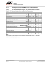
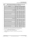
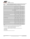
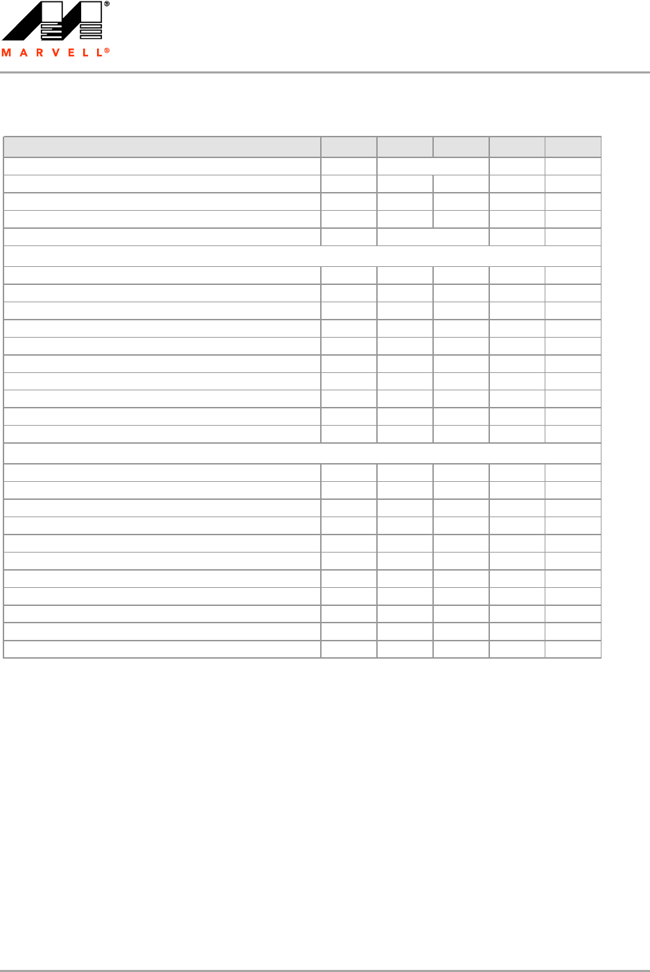
8.7.3.2 SATA-II Interface Gen2i Mode Driver and Receiver Characteristics
Table 68: SATA-II Interface Gen2i Mode Driver and Receiver Characteristics
Description Symbol Min Max Units Notes
Baud Rate BR Gbps -
Baud rate tolerance Bppm -350.0 350.0 ppm -
Spread spectrum modulation frequency Fssc 30.0 33.0 kHz -
Spread spectrum modulation Deviation SSCtol -5000.0 0.0 ppm -
Unit Interval UI ps -
Output differential voltage Vdifftx 400.0 700.0 mV 1 , 2
Differential return loss (150 MHz-300 MHz) RLOD 14.0 - dB -
Differential return loss (300 MHz-600 MHz) RLOD 8.0 - dB -
Differential return loss (600 MHz-2.4 GHz) RLOD 6.0 - dB -
Differential return loss (2.4 GHz-3.0 GHz) RLOD 3.0 - dB -
Differential return loss (3.0 GHz-5.0 GHz) RLOD 1.0 - dB -
Total jitter at connector clock-data TJ10 - 0.30 UI 3
Deterministic jitter at connector clock-data DJ10 - 0.17 UI 3
Total jitter at connector clock-data TJ500 - 0.37 UI 4
Deterministic jitter at connector clock-data DJ500 - 0.19 UI 4
Input differential voltage Vdiffrx 275.0 750.0 mV 5
Differential return loss (150 MHz-300 MHz) RLID 18.0 - dB -
Differential return loss (300 MHz-600 MHz) RLID 14.0 - dB -
Differential return loss (600 MHz-1.2 GHz) RLID 10.0 - dB -
Differential return loss (1.2 GHz-2.4 GHz) RLID 8.0 - dB -
Differential return loss (2.4 GHz-3.0 GHz) RLID 3.0 - dB -
Differential return loss (3.0 GHz-5.0 GHz) RLID 1.0 - dB -
Total jitter at connector clock-data TJ10 - 0.46 UI 3
Deterministic jitter at connector clock-data DJ10 - 0.35 UI 3
Total jitter at connector clock-data TJ500 - 0.60 UI 4
Deterministic jitter at connector clock-data DJ500 - 0.42 UI 4
Note s:
General Comment: For more information, refer to SATA II Revision 2.6 Specification, February, 2007.
General Comment: The load is 100 ohm differential for these parameters, unless otherw ise specified.
General Comment: To comply w ith the values presented in this table, refer to your local
Marvell representative for register settings.
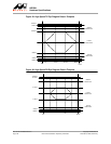
1. 0.45-0.55 UI is the range w here the signal meets the minimum level.
2. Output Differential Amplitude and Pre-Emphasis are configurabile. See functional register description
for more details.
3. Defined for BR/10.
4. Defined for BR/500.
5. 0.5 UI is the point where the signal meets the minimum level.
Driver Parameters
Receiver Parameters
333.33
3.0


