Electrical Specifications
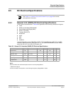
AC Electrical Specifications
Copyright © 2008 Marvell Doc. No. MV-S104859-U0 Rev. E
December 2, 2008, Preliminary Document Classification: Proprietary Information Page 89
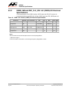
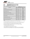
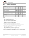
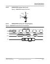
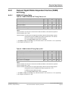
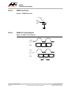
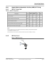
Table 47: SDRAM DDR2 Interface Address Timing Table
Min Max
Address and Control valid output time before CLK-CLkn rising edge tAOVB 0.65 - ns 1, 2
Address and Control valid output time after CLK-CLKn rising edge tAOVA 0.65 - ns 1, 2
Address and Control valid output time before CLK-CLkn rising edge tAOVB 2.95 - ns 1, 3
Address and Control valid output time after CLK-CLKn rising edge tAOVA 0.65 - ns 1, 3
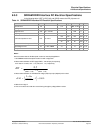
Notes:
General comment: All timing values were measured from vref to vref, unless otherwise specified.
General comment: For all signals, the load is CL = 14 pF.
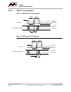
1. This timing value is defined on CLK / CLKn crossing point.
2. This timing value is defined when Address and Control signals are output on CLK-CLKn falling edge.
For more information, see register settings.
3. This timing value is defined when Address and Control signals are output on CLK-CLKn falling edge.
and 2T mode is enabled. For more information, see register settings.
Except for ODT, CKE and CS signals.
Note sDe scr iption Sym bol
400 MHz @ 1.8V
Units


