


Appendix D Register-Level Programming
PC-LPM-16/PnP User Manual D-30
National Instruments Corporation
Clearing the Analog Input Circuitry
Write to the A/D Clear Register to clear the analog input circuitry,
which leaves the analog input circuitry in the following state:
• Analog input error flag OVERFLOW is cleared.
• Pending interrupt requests are cleared.
To empty the A/D FIFO before starting any A/D conversions, perform
two 8-bit reads on the A/D FIFO Registers and ignore the data read.
This operation guarantees that the A/D conversion results read from the
A/D FIFO are from the initiated conversions rather than leftover results
from previous conversions.
To clear the analog input circuitry and the A/D FIFO:
• Write 0 to the A/D Clear Register (8-bit write).
Programming Multiple A/D Conversions on a Single Input Channel Using
Counter 0
This manual refers to a sequence of timed A/D conversions as a data
acquisition operation. Counter 0 of the MSM82C53 is used as the
sample-interval counter. In a data acquisition operation, counter 0
continuously generates the conversion pulses. The software keeps track
of the number of conversions that have occurred and turns off counter 0
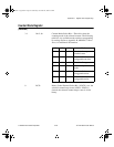
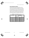
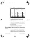
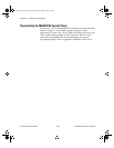
Table D-3. Bipolar Input Mode A/D Conversion Values
Input Voltage A/D Conversion Result
Range: -5 to +5 V
(13-bit values)
A/D Conversion Result
Divided by 2
(12-bit values)
(Decimal) (Hex) (Decimal) (Hex)
-5.0 -4,096 F000 -2,048 F800
-2.5 -2,048 F800 -1,024 FC00
0 0 0000 0 0000
2.5 2,048 0800 1,024 0400
4.9976 4,095 0FFF 2,047 07FF
a.Book : l.Appendix D Page 30 Wednesday, November 20, 1996 6:36 PM