


Chapter 4 Signal Connections
PC-LPM-16/PnP User Manual 4-12
National Instruments Corporation
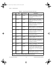
MSM82C53 digital input specifications (referenced to DGND):
•V
IH
input logic high voltage 2.2 V min
•V
IL
input logic low voltage 0.8 V max
• Input load current
±
10.0
µ
A max
MSM82C53 digital output specifications (referenced to DGND):
•V
OH
output logic high voltage 3.7 V min
•V
OL
output logic low voltage 0.45 V max
•I
OH
output source current, at V
OH
1.0 mA max
•I
OL
output sink current, at V
OL
4.0 mA max
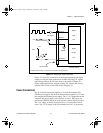
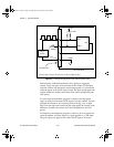
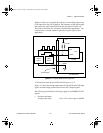
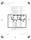
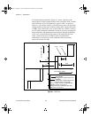
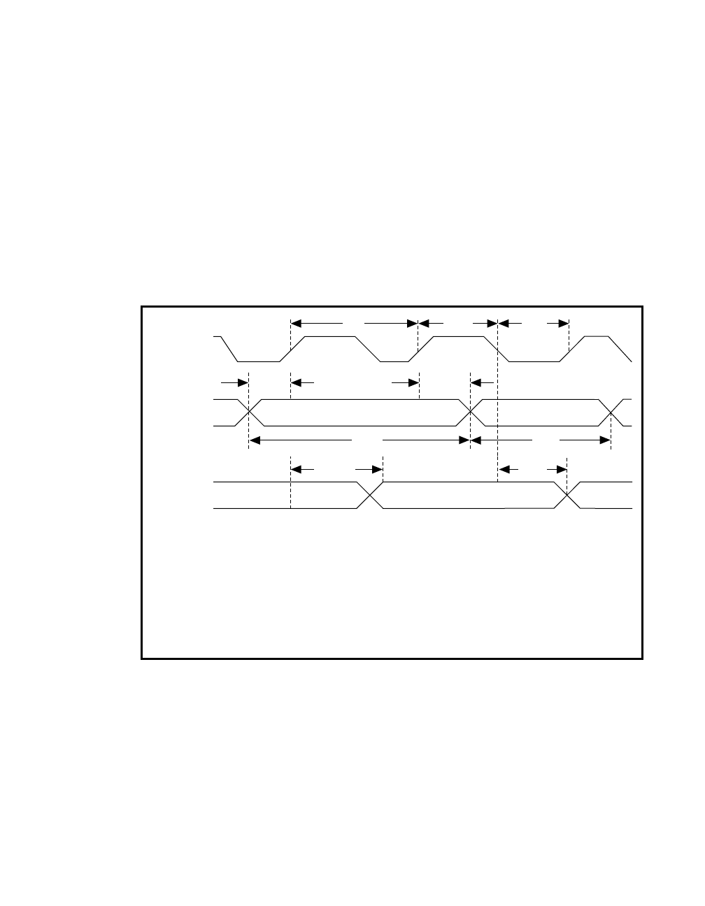
Figure 4-7.
General-Purpose Timing Signals
The GATE and OUT signals in Figure 4-7 are referenced to the rising
edge of the CLK signal.
t
outc
t
gwl
t
gwh
t
sc
V
IH
V
IL
V
IH
V
IL
V
OH
V
OL
t
pwh
t
pwl
t
gh
t
gsu
t
outg
t
sc
clock period 125 ns min
t
pwh
clock high level 60 ns min
t
pwl
clock lowlevel 60 ns min
t
gsu
gate setup time 60 ns min
t
gh
gate hold time 60 ns min
t
gwh
gate high level 60 ns min
t
gwl
gate low level 60 ns min
t
outg
output delay from clock 60 ns min
t
outc
output delay from gate 60 ns min
CLK
GATE
OUT
a.Book : h.chapter 4 Page 12 Wednesday, November 20, 1996 6:36 PM