


Chapter 3 Theory of Operation
National Instruments Corporation 3-9 PC-LPM-16/PnP User Manual
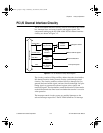
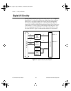
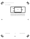
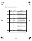
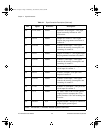
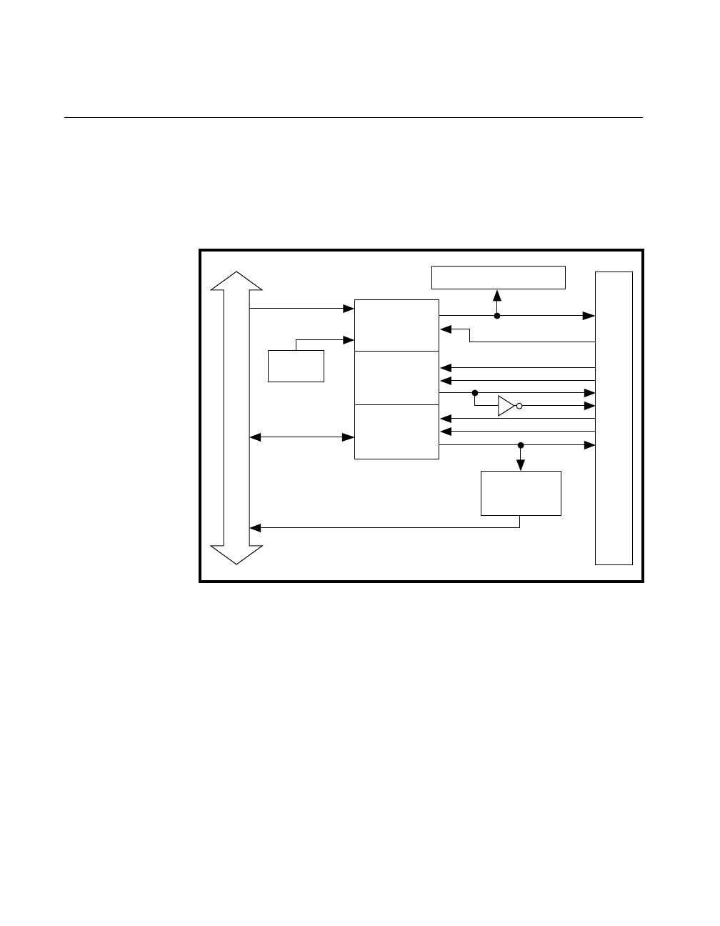
Timing I/O Circuitry
The PC-LPM-16PnP uses an MSM82C53 Counter/Timer integrated
circuit for data acquisition timing and for general-purpose timing I/O
functions. Three counters on the circuit are available for general use,
but the board can use only one of them, counter 0, internally for data
acquisition timing. Figure 3-5 shows a block diagram of both groups of
timing I/O circuitry.
Figure 3-5.
Timing I/O Circuitry Block Diagram
The MSM82C53 contains three independent 16-bit counter/timers and
one 8-bit Mode Register. As shown in Figure 3-5, you can use counter 0
for data acquisition timing, and counters 1 and 2 are free for general use.
You can program all three counter/timers to operate in several useful
timing modes. The programming and operation of the MSM82C53 is
presented in detail both in Appendix B,
MSM82C53 Data Sheet
, and
Appendix D,
Register-Level Programming
.
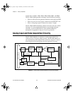
The timebase for counter 0 uses a 1 MHz clock generated from an
onboard oscillator. You must externally supply the timebases for
counters 1 and 2 through the 50-pin I/O connector. Figure 3-6 diagrams
the 16-bit counters in the MSM82C53.
PC I/O Channel
OUT0
GATE0
CLK1
GATE1
OUT1
CLK2
GATE2
OUT2
1 MHz
Clock
8
/
Data
OUT0
GATE0
CLK1
GATE1
OUT1
OUT1*
CLK2
GATE2
OUT2
I/O Connector
CLK0
A/D Conversion Logic
CTR RD/WR
MSM82C53
Counter/Timer
Plug and Play
Interrupt
Interface
a.Book : g.chapter 3 Page 9 Wednesday, November 20, 1996 6:36 PM