


www.ti.com
2.4.4READCommand
DDR_CLK
DDR_CKE
DDR_CS
DDR_WE
DDR_CAS
DDR_DQM[3:0]
DDR_D[31:0]
DDR_A[12:0]
DDR_RAS
DDR_DQS[3:0]
COL
BANK
DDR_A[10]
DDR_BA[2:0]
CAS Latency
D0 D1 D2 D3 D4 D5 D6 D7
DDR_CLK
PeripheralArchitecture
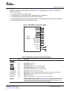
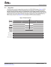
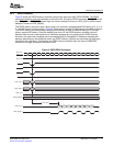
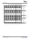
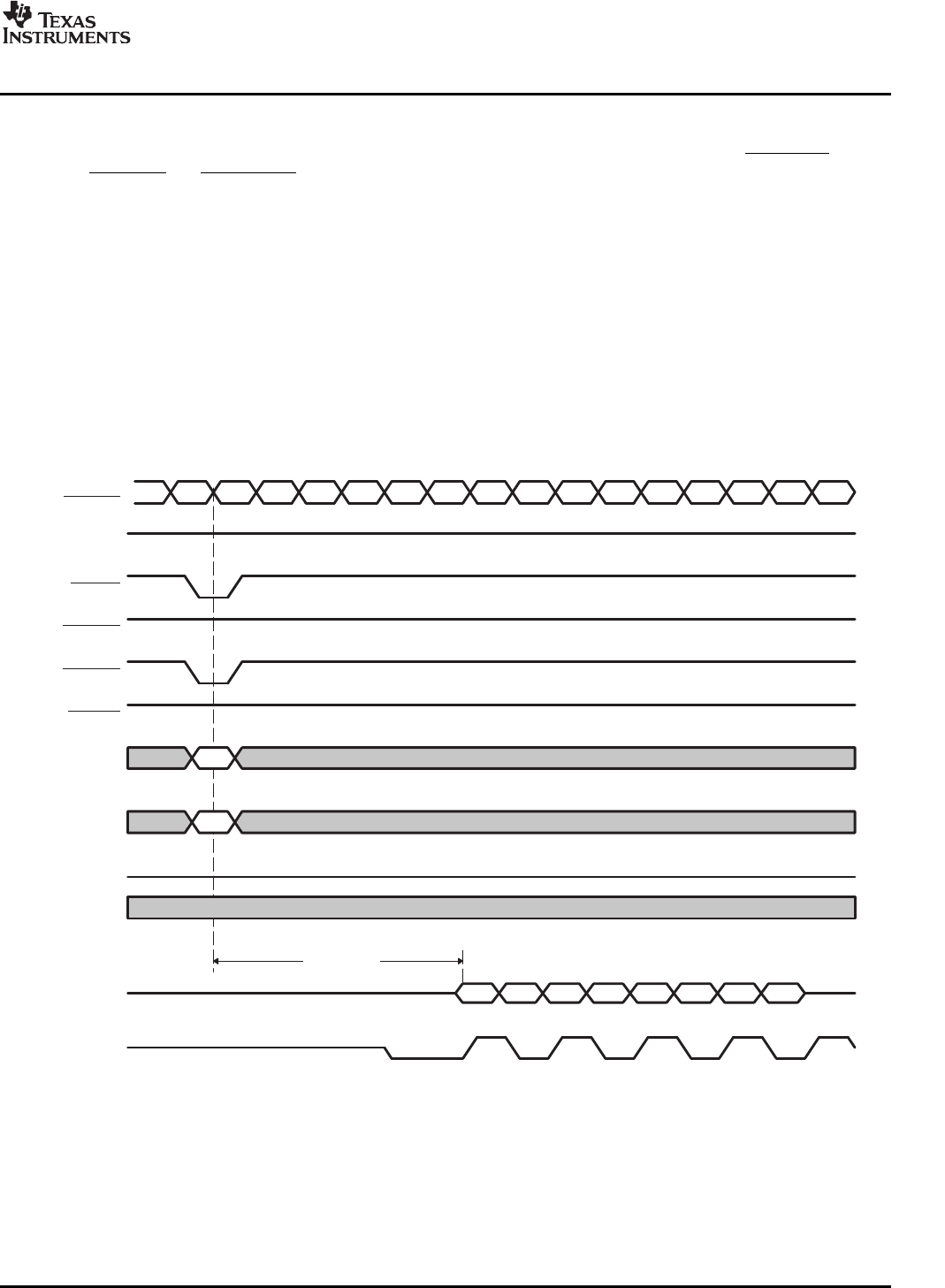
Figure8showstheDDR2memorycontrollerperformingareadburstfromDDR2SDRAM.TheREAD
commandinitiatesaburstreadoperationtoanactiverow.DuringtheREADcommand,DDR_CASdrives
low,DDR_WEandDDR_RASremainhigh,thecolumnaddressisdrivenonDDR_A[12:0],andthebank
addressisdrivenonDDR_BA[2:0].
TheDDR2memorycontrollerusesaburstlengthof8,andhasaprogrammableCASlatencyof2,3,4,or
5.TheCASlatencyisthreecyclesinFigure8.ReadlatencyisequaltoCASlatencyplusadditivelatency.
TheDDR2memorycontrolleralwaysconfiguresthememorytohaveanadditivelatencyof0,soread
latencyequalsCASlatency.Sincethedefaultburstsizeis8,theDDR2memorycontrollerreturns8
piecesofdataforeveryreadcommand.IfadditionalaccessesarenotpendingtotheDDR2memory
controller,thereadburstcompletesandtheunneededdataisdisregarded.Ifadditionalaccessesare
pending,dependingontheschedulingresult,theDDR2memorycontrollercanterminatethereadburst
andstartanewreadburst.Furthermore,theDDR2memorycontrollerdoesnotissueaDAB/DEAC
commanduntilpageinformationbecomesinvalid.
Figure8.DDR2READCommand
SPRU986B–November2007DDR2MemoryController17
SubmitDocumentationFeedback