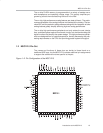
MSC1210 Pin-Out
1-4
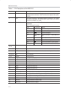
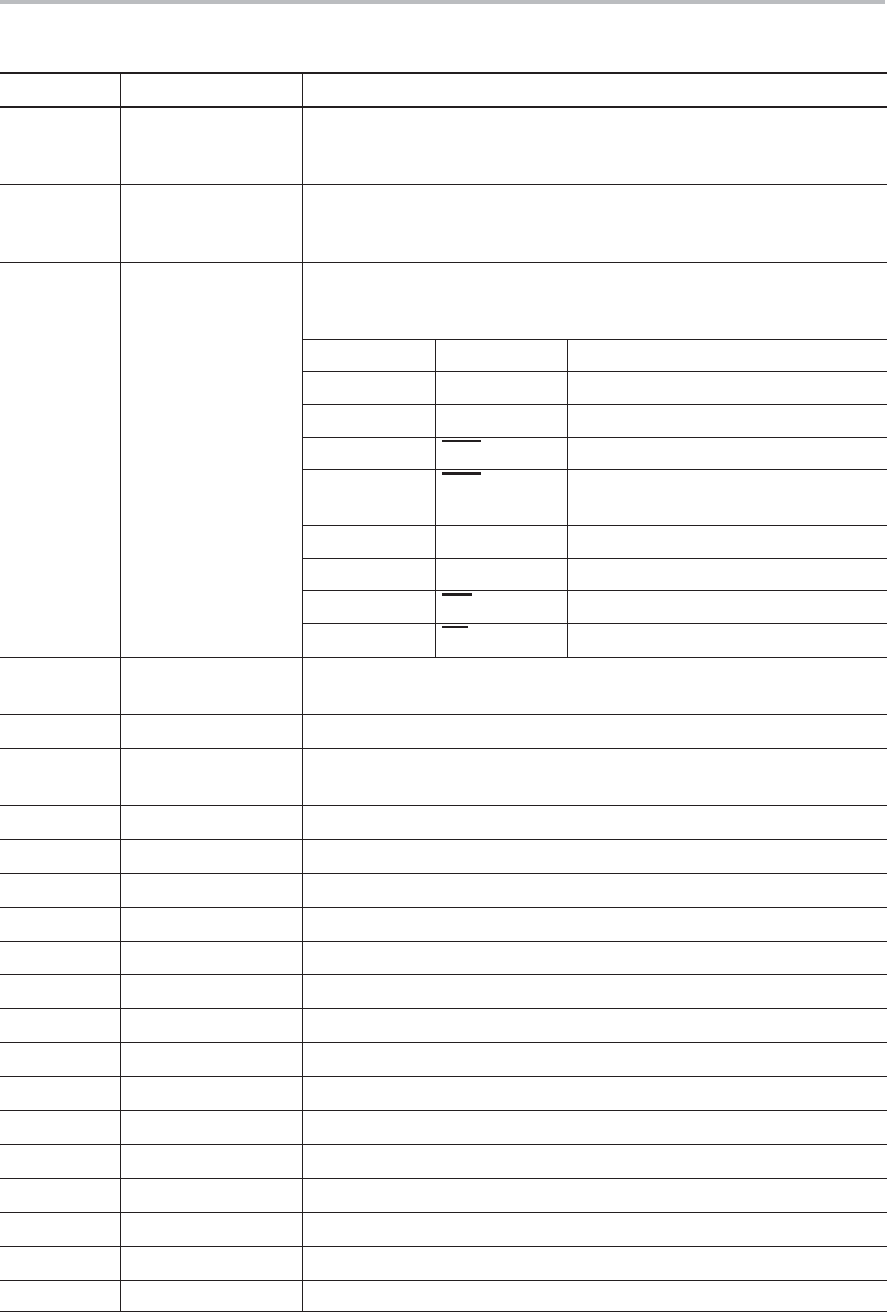
Table 1−1.Pin Descriptions of the MSC1210
Pin # Name Description
1 XOUT The crystal oscillator pin XOUT supports parallel resonant AT cut crys-
tals and ceramic resonators. XOUT serves as the output of the crystal
amplifier.
2 XIN The crystal oscillator pin XIN supports parallel resonant AT cut crystals
and ceramic resonators. XIN can also be an input if there is an external
clock source instead of a crystal.
3-10 P3.0-P3.7 Port 3 is a bidirectional I/O port. The alternate functions for Port3 are
listed below.
Port 3—Alternate Functions:
PORT ALTERNATE MODE
P3.0 RxD0 Serial Port 0 Input
P3.1 TxD0 Serial Port 0 Output
P3.2 INT0 External Interrupt 0
P3.3 INT1/TONE/
PWM
External Interrupt 1/TONE/PWM Out-
put
P3.4 T0 Timer 0 External Input
P3.5 T1 Timer 1 External Input
P3.6 WR External Data Memory Write Strobe
P3.7 RD External Data Memory Read Strobe
11, 14, 15,
42, 58
DV
DD
Digital Power Supply
12, 41, 57 DGND Digital Ground
13 RST A HIGH on the reset input for two instruction clock cycles will reset the
device.
16, 32, 33 NC No Connection
17, 27 AGND Analog Ground
28 AV
DD
Analog Power Supply
18 AIN0 Analog Input Channel 0
19 AIN1 Analog Input Channel 1
20 AIN2 Analog Input Channel 2
21 AIN3 Analog Input Channel 3
22 AIN4 Analog Input Channel 4
23 AIN5 Analog Input Channel 5
24 AIN6, EXTD Analog Input Channel 6, Digital Low Voltage Detect Input
25 AIN7, EXTA Analog Input Channel 7, Analog Low Voltage Detect Input
26 AINCOM Analog Common for Single−Ended Inputs
29 REF IN– Voltage Reference Negative Input
30 REF IN+ Voltage Reference Positive Input
31 REF OUT Voltage Reference Output


