Internal RAM
2-7
MSC1210 Memory Organization
2.4.1 The Stack
The stack is a “last in, first out” (LIFO) storage area that exists in internal RAM.
It is used by the MSC1210 to store values that the user program manually
pushes onto the stack, as well as to store the return addresses for CALLs and
interrupt service routines (ISRs)—more on these topics later.
The stack is defined and controlled by an SFR called SP. As a standard 8−bit
SFR, SP holds a value between 0 and 255 that represents the internal RAM
address of the end of the current stack. If a value is removed from the stack,
it is taken from the internal RAM address pointed to by SP, and SP will subse-
quently be decremented by 1. If a value is pushed onto the stack, SP is first
incremented and then the value is inserted in internal RAM at the address now
pointed to by SP.
SP is initialized to 07
H
when the MSC1210 is first powered up. This means the
first value to be pushed onto the stack is placed at internal RAM address 08
H
(07
H
+ 1), the second is placed at 09
H
, etc.
Note:
By default, the MSC1210 initializes the stack pointer (SP) to 07
H
when the
microcontroller is reset. This means that the stack will start at address 08
H
and expand upwards. If using the alternate register banks (banks 1, 2, or 3)
the stack pointer must be initialized to an address above the highest register
bank being used. Otherwise, the stack will overwrite the alternate register
banks. Similarly, if using bit variables, it is usually a good idea to initialize the
stack pointer to some value greater than 2F
H
to ensure that the bit variables
are protected from the stack. Following is more information about the register
banks and bit memory.
2.4.2 Register Banks
The MSC1210 uses eight R registers, which are used in many of its instructions.
These R registers are numbered from 0 through 7 (R0, R1, R2, R3, R4, R5, R6,
and R7) and are generally used to assist in manipulating values and moving data
from one memory location to another. For example, to add the value of R4 to the
accumulator, the following assembly language instruction would be executed:
ADD A,R4
Thus, if the accumulator (A) contains the value 6, and R4 contains the value 3,
the accumulator will contain the value 9 after this instruction is executed.
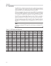
However, as the memory map of Figure 2−2 illustrates, R Register R4 is really
part of internal RAM. Specifically, R4 is address 04
H
of internal RAM. This can
be seen in the bright green section of the memory map. The above instruction,
therefore, accomplishes the same thing as the following operation:
ADD A,04h
This instruction adds the value found in internal RAM address 04
H
to the value
of the accumulator, leaving the result in the accumulator. The above instruction
effectively accomplishes the same thing as the previous ADD instruction be-
cause R4 is really internal RAM address 04
H
.


