Analog-to-Digital Converter
17-17
Keil Simulator
17.7 Analog-to-Digital Converter
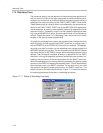
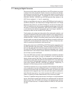
Data entry and bit pattern setting facilities for the ADC peripheral are similar
to those of the other peripherals. Some of the text entry boxes are editable,
while others are just read-only, and the check boxes respond to mouse clicks
with checked and cleared status. The editable text entry windows marked
ADCON0, ADCON1, ADCON2 and ADCON3 provide direct access to the
ADC Control registers 0, 1, 2 and 3, respectively.
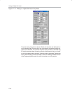
Writing to the editable text entry box marked ADCON0 sets the bit pattern for
the Burnout Detect bit, the Enable Internal Voltage Reference bit, the Voltage
Reference High Select bit, the Buffer Enable bit, and the bits that select the
PGA. All these bits could also be set or modified by performing a check/clear
activation on check boxes marked BOD, VREF, BUF and VREFH, respective-
ly, and selecting the desired programmable gain from the gain selection list
that pops up when the box marked PGA is activated.
The bit patterns for analog input data polarity, filter mode option selection, and
the device’s calibration mode control option selection can be programmed or
updated by entering appropriate byte data values into the editable text box
marked ADCON1. Similarly, the polarity setting and the filter settling mode
selection option can also be programmed, alternatively, through the check box
marked POL and the selection box marked Filter. There is no data entry alter-
native for selecting the calibration mode control bits.
Writing data values into the ADCON2 and ADCON3 registers respectively sets
the ADC decimation filter ratio values. The lower three bits of ADCON3 corre-
spond to the most significant three bits of the converter decimation ratio, and
the whole ADCON2 byte represents the LSB for the decimation ratio. It should
be stressed that if the contents of either ADCON2 or ADCON3 are modified,
the converter must be recalibrated.
The current ADC data conversion rate is automatically computed on the basis
of the system clock setting. Its result is displayed in the non-editable text
display window marked Data Rate. The data conversion completed status, is
indicated by the logic state of the ADC bit of the AISTAT SFR. The 24-bit result
of the most recent analog-to-digital conversion, which is a concatenation of the
three result registers ADRESH, ADRESM and ADRESL, respectively, is
displayed in the text display window marked ADRESH/M/L.
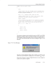
The MSC1210 device has an input multiplexer which facilitates the selection
of any combination of any pair of differential inputs. If you select any of the input
channels for the positive input of the differential input pair, any other input could
be selected for the negative input. Even, the same input could be selected for
both differential input pairs, if you wishe to perform the ADC conversion cal-
ibration or quantify the noise measurements of the conversion system.
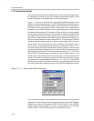
There are 10 possible analog input sources, including an on-chip temperature
sensor. Activating the analog input selection box associated with the pertinent
differential pair input, INP or INN, and clicking on the desired source could se-
lect any of these channels. The default selection for AIN0 for INP, and AIN1
for INN.


