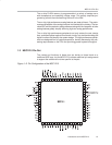
MSC1210 Pin-Out
1-5
Introduction to the MSC1210
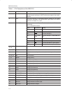
Table 1−1 Pin Descriptions of the MSC1210 (Continued)
Pin # Name Description
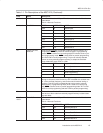
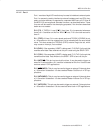
34-40, 43 P2.0-P2.7 Port 2 is a bidirectional I/O port. The alternate functions for Port 2 are
listed below.
Port 2—Alternate Functions:
34-40, 43 P2.0-P2.7 PORT ALTERNATE MODE
P2.0 A8 Address Bit 8
P2.1 A9 Address Bit 9
P2.2 A10 Address Bit 10
P2.3 A11 Address Bit 11
P2.4 A12 Address Bit 12
P2.5 A13 Address Bit 13
P2.6 A14 Address Bit 14
P2.7 A15 Address Bit 15
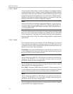
44 PSEN, OSCCLK,
MODCLK
Program Store Enable: Connected to optional external memory as a
chip enable. PSEN
will provide an active low pulse. In programming
mode, PSEN
is used as an input along with ALE to define serial or par-
allel programming mode. PSEN
is held HIGH for parallel programming
and tied LOW for serial programming. This pin can also be selected
(when not using external program memory) to output the Oscillator
clock, Modulator clock, HIGH, or LOW.
ALE PSEN Program Mode Selection
NC NC Normal Operation
0 1 Parallel Programming
1 0 Serial Programming
0 0 Reserved
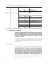
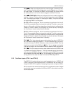
45 ALE Address Latch Enable: Used for latching the low byte of the address
during an access to external memory. ALE is emitted at a constant rate
of 1/2 the oscillator frequency, and can be used for external timing or
clocking. One ALE pulse is skipped during each access to external
data memory. In programming mode, ALE is used as an input along
with PSEN
to define serial or parallel programming mode. ALE is held
HIGH for serial programming and tied LOW for parallel programming.
48 EA External Access Enable: EA must be externally held LOW to enable
the device to fetch code from external program memory locations start-
ing with 0000
H
.
46, 47,
49-54
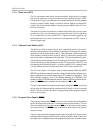
P0.0−P0.7 Port 0 is a bidirectional I/O port. The alternate functions for Port 0 are
listed below.
Port 0—Alternate Functions:
PORT ALTERNATE MODE
P0.0 AD0 Address/Data Bit 0
P0.1 AD1 Address/Data Bit 1
P0.2 AD2 Address/Data Bit 2
P0.3 AD3 Address/Data Bit 3
P0.4 AD4 Address/Data Bit 4


