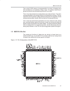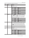
MSC1210 Pin-Out
1-9
Introduction to the MSC1210
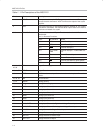
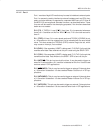
P3.2 (INT0): When so configured, this line is used to trigger an external 0 Inter-
rupt. This may either be low-level triggered or may be triggered on a 1-0 transi-
tion (see Chapter 10, Interrupts, for details). You can assign any function to this
pin as long as the circuit has no need to trigger an external 0 interrupt.
P3.3 (INT1
/TONE/PWM): When so configured, this line is used to trigger an
external 1 Interrupt. This may either be low-level triggered or may be triggered
on a 1-0 transition (see Chapter 10, Interrupts, for details). This pin is also used
for outputting PWM, if so configured.
P3.4 (T0): When so configured, this line is used as the clock source for timer 0.
Timer 0 is incremented either every instruction cycle that T0 is high, or every time
there is a 1-0 transition on this line, depending on how the timer is configured (see
Chapter 8, Timers, for details). You can assign any function to this pin as long as
the circuit has no need to control timer 0 externally.
P3.5 (T1): When so configured, this line is used as the clock source for timer 1.
Timer 1 is incremented either every instruction cycle that T1 is high, or every time
there is a 1-0 transition on this line, depending on how the timer is configured (see
Chapter 8, Timers, for details). You can assign any function to this pin as long as
the circuit has no need to control timer 1 externally.
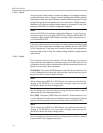
P3.6 (WR
): This is the external memory write strobe line when bit EGP23 is
set in hardware configuration Register 1. This line is asserted low by the micro-
controller whenever a MOVX instruction writes to external RAM. This line
should be connected to the RAM write (W
) line. You can assign any function
to this pin as long as the circuit does not write to external RAM using MOVX.
P3.7 (RD
): This is the external memory read strobe line when bit EGP23 is set
in hardware configuration Register 1. This line is asserted low by the microcon-
troller whenever a MOVX instruction is read from external RAM. This line must
be connected to the RAM read (R
) line. You can assign any function to this pin
as long as the circuit does not read from external RAM using MOVX.
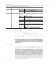
1.2.2 Oscillator Inputs (XTAL1 and XTAL2)
The MSC1210 is typically driven by a crystal connected to pins 1 (XOUT) and
2 (XIN). Common crystal frequencies are 11.0592MHz as well as 12MHz, al-
though the MSC1210 is capable of accepting frequencies as high as 33MHz.
While a crystal is the normal clock source, this is not always the case. A digital
clock source may also be attached to XIN and XOUT to provide the clock for
the microcontroller.


